
Hitachi, Ltd. (hereafter, Hitachi), Kyushu University, National Research and Development Corporation RIKEN (hereafter, RIKEN), and HREM Co., Ltd. are collaborating with the National Institute of Advanced Industrial Science and Technology and the National Institute for Materials Research to develop a method that enables magnetic field observation of samples with uneven structure or composition, such as magnetic multilayer films (hereafter, heterogeneous samples*1), which have been difficult to observe until now, using Hitachi's atomic resolution/holography electron microscopes, For the first time in the world, we have successfully observed magnetic fields on each lattice surface*2.
This result was achieved by improving the accuracy of electron holography and developing a technology to automatically correct focus after imaging. This made it possible for the first time to observe magnetic fields at the atomic layer level at the boundary (interface) between local materials, which greatly affects the physical properties of materials containing heterogeneous samples and the characteristics of electronic devices. In the future, we will contribute to the development of basic science through elucidation of magnetic phenomena*3 occurring at the atomic layer level, and we will contribute to the development of high-performance magnets and high-performance materials for electrification for decarbonization, and the development of energy-saving devices to reduce overall energy consumption required in everyday life in order to realize a carbon-neutral society.
Note, the results of this research were published online in the international journal “Nature” on Thursday, July 4, 2024 at midnight (Japan time) *4.
Research background
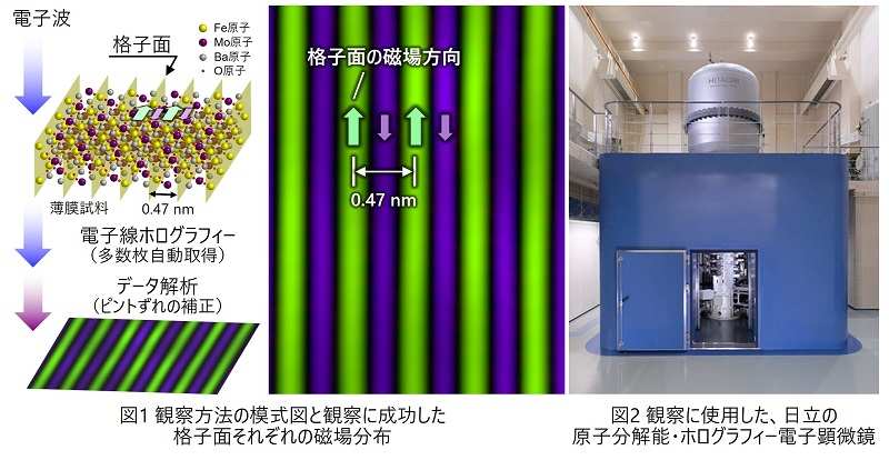
Electronic devices and motors are used in various applications such as smartphones, computers, automobiles, railways, and power plants, and support our daily lives. Since most of these functions and properties are related to the arrangement of atoms and the behavior of electrons, which are the smallest units of matter, there is a need for technology to observe matter with ultra-high resolution at the atomic level in order to develop new functions and further improve performance. Until now, Hitachi has been developing holography electron microscopes since 1966 in order to directly observe electric and magnetic fields in minute regions, and developed an atomic resolution/holography electron microscope in 2014 with a grant from the “Advanced Research and Development Support Program (FIRST)” (FIRST) (Figure 2). In 2017, in collaboration with RIKEN, we achieved a resolution of 1 nm*5 or less, which enables magnetic field observation in atomic number layers*6. However, improving the accuracy of microscopes and correcting minute focus deviations that occur during imaging were issues in order to further increase resolution.
Therefore, this time, the joint research team solved these issues and developed a technology that realizes magnetic field observation on each lattice surface for heterogeneous samples such as magnetic multilayer films, which have been difficult to observe until now.
Features of development technology
- High-volume automatic image acquisition technology to improve the accuracy of electron holography
The accuracy of electron holography is improved by increasing the number of image data to be acquired. Based on technology that separates electric field information from magnetic field information with high accuracy from electron holography observation results developed in 2017, we have developed a technology that automatically acquires 10,000 images or more in about 8.5 hours by automatically controlling and adjusting the microscope during data acquisition and speeding up shooting. - Digital aberration correction technology that automatically corrects minute misalignment
In order to obtain high resolution, technology is necessary to correct minute focus deviations left in the imaging data. The idea of correcting focus after imaging is the very motivation of Dennis Gabor when he invented electron holography in 1948, and although it was theoretically established, there has been no technology for automatic correction until now. This time, we succeeded in automatic correction by applying a method*7 for correcting focus by analyzing electron waves obtained by changing focus to electron beam holography and developing a unique algorithm to reduce the effects of noise included in experimental data.
By applying this technology to an atomic resolution/holography electron microscope, we observed magnetic materials (Ba2FeMoO6 crystals) with magnetic fields of different sizes and directions for each atomic layer, and as a result of comparison and examination with simulations, we succeeded in observing the magnetic field of each lattice surface inside the material with a resolution of 0.47 nm, which is the world's highest performance*8 as a method for observing samples that are not uniform.
With these results, it is now possible to observe in detail the relationship between interface structures in devices and materials and magnetic fields, and it is expected that development of high-performance materials and energy-saving devices will be accelerated to realize a carbon-neutral society in the future. Furthermore, through support from the Ministry of Education, Culture, Sports, Science and Technology's Advanced Research Infrastructure Sharing Promotion Project, we will jointly use this device and contribute to the development of science and technology in a wide range of fields, from basic physics to cutting-edge devices.
Comment from Yoshinori Tokura Group Director, Strong Correlation Condensed Matter Research Group, RIKEN Center for Emergent Matter Science
This result is a new electron microscopy method that can directly observe magnetic fields at the lattice surface level, and is expected to contribute to the development of material science. In the future, I am convinced that utilizing this method will pave the way for innovative electronics principle construction and device development that greatly suppresses power loss.
In addition, part of this research is funded through the Japan Society for the Promotion of Science (Chairman: Sugino Tsuyoshi) through a cutting-edge research and development support program, and strategic creative research promotion project team type research (CREST) “Development and application of intelligent measurement/analysis methods through the fusion of measurement technology and advanced information processing” (Research Summary: Amemiya Yoshiyuki, Special Professor of Frontier Sciences, Graduate School of Frontier Sciences, University of Tokyo) It received support for the research project “Technological Innovation in Electron Microscopy Using AI and Large-Scale Image Processing (JPMJCR1664)” (Research Representative: Murakami Kyokazu, Professor, Kyushu University Graduate School of Engineering, Research Period: Heisei 28 to Reiwa 2).
Introduction to Hitachi's atomic resolution holography electron microscopes
- Overview explanation
- Introduction video
- 2015/2/18 Hitachi News Release
“We developed an atomic resolution holography electron microscope and achieved the world's highest resolution of 43 picometers”
About Hitachi, Ltd.
Hitachi is promoting social innovation projects that realize a sustainable society through data and technology. We solve customer and social issues through Lumada solutions that utilize IT, OT (control/operation technology), and products under a three-sector business system: “digital systems & services” that support customer DX; “green energy & mobility” that contributes to the realization of a decarbonized society through energy and railways; and “Connected Industries,” which digitally connects products in a wide range of industries and provides solutions . Driven by digital, green, and innovation, we aim for growth through co-creation with customers. Sales revenue for the three sectors in fiscal 2023 (fiscal year ending 2024/3) was 8,564.3 billion yen, and as of the end of 2024/3, there are 573 consolidated subsidiaries and approximately 270,000 employees worldwide.
- Hitachi website
- About Lumada
Contact information
Hitachi, Ltd. Research and Development Group
- Go to the research and development inquiry form
National University Corporation Kyushu University
PR Division
Phone: 092-802-2130
- E-mail: koho@jimu.kyushu-u.ac.jp
National Research and Development Corporation RIKEN
Public Relations Office Press Officer
Phone: 050-3495-0247
- E-mail: ex-press@ml.riken.jp
HREM Co., Ltd. (HREM Research Inc.)
- E-mail: support@hremresearch.com
The information described in this news release (product price, product specifications, service details, release date, contact information, URL, etc.) is current as of the announcement date. Please note that changes are made without notice, and the search date and information may differ. Please see the list of inquiries for the latest contact information.