
COHERENT ANNOUNCES THE WORLD'S FIRST 6-INCH INDIUM PHOSPHIDE SCALABLE WAFER FABS PAVING THE WAY FOR THE NEXT GENERATION OF LASERS FOR AI TRANSCEIVERS AND 6G WIRELESS NETWORKS
COHERENT ANNOUNCES THE WORLD'S FIRST 6-INCH INDIUM PHOSPHIDE SCALABLE WAFER FABS PAVING THE WAY FOR THE NEXT GENERATION OF LASERS FOR AI TRANSCEIVERS AND 6G WIRELESS NETWORKS
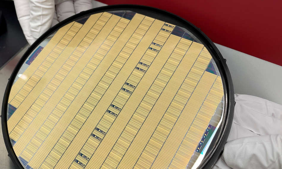
PITTSBURGH, March 25, 2024 (GLOBE NEWSWIRE) – Coherent Corp. (NYSE: COHR), a leading provider of compound semiconductors and high-performance optical networking solutions, announced today it has established the world's first capability for 6-inch indium phosphide (InP) wafer fabrication, in the company's Sherman, Texas, and Järfälla, Sweden, wafer fabs. This exciting milestone enables Coherent to increase production capacity and lower die costs for InP optoelectronic devices, widely used in applications such as coherent optical communications, datacom transceivers, AI interconnects, advanced sensing for consumer electronics and wearables, medical and automotive applications, and, in the future, in 6G wireless and satellite communications networks.
匹茲堡,2024年3月25日(GLOBE NEWSWIRE)——複合半導體和高性能光網絡解決方案的領先提供商Coherent Corp.(紐約證券交易所代碼:COHR)今天宣佈,它已在該公司的德克薩斯州謝爾曼和瑞典賈爾法拉的晶圓廠建立了世界上第一個6英寸磷化銻(InP)晶圓製造能力。這一激動人心的里程碑使Coherent能夠提高InP光電子器件的產能並降低芯片成本,這些器件廣泛用於相干光通信、數據通信收發器、人工智能互連、消費電子和可穿戴設備的高級傳感、醫療和汽車應用以及未來的6G無線和衛星通信網絡等應用。
"We are very excited to announce our 6-inch indium phosphide wafer fabrication capability in both our Sherman and Järfälla fabs, which is a result of our continuous investment in innovation and technology development, and our years of investment and operating experience in high-volume VCSEL array manufacturing for mobile handsets," said Dr. Giovanni Barbarossa, Chief Strategy Officer and President, Materials Segment. "Vertical integration at scale is a core strategy that we have been relying upon in several of our markets, and it has enabled our optoelectronics products to win in the marketplace by delivering world-class quality, performance, time-to-market, and cost advantage."
材料部門首席戰略官兼總裁喬瓦尼·巴巴羅薩博士表示:“我們非常高興地宣佈,我們在謝爾曼和賈爾法拉晶圓廠均有6英寸磷化銦晶圓製造能力,這是我們對創新和技術開發的持續投資,以及我們在手機大批量VCSEL陣列製造方面多年的投資和運營經驗的結果。”“大規模垂直整合是我們在多個市場中一直依賴的核心戰略,它通過提供世界一流的質量、性能、上市時間和成本優勢,使我們的光電子產品能夠在市場上獲勝。”
"Moving to 6-inch wafers will enable us to continue to deliver massive productivity improvements, including manufacturing 4x the number of devices per wafer, achieve a greater than 60% reduction in die cost, and allow us to transition our fabs to higher-capacity, more-efficient automated process tools," said Dr. Beck Mason, Executive Vice President, Telecommunications. "This capability will allow us to meet the growing demand for our indium phosphide products in several of our core markets, while enhancing our competitiveness and profitability."
電信執行副總裁貝克·梅森博士表示:“轉向6英寸晶圓將使我們能夠繼續大幅提高生產率,包括生產每晶圓數量的4倍,芯片成本降低60%以上,並使我們能夠將晶圓廠過渡到容量更大、效率更高的自動化工藝工具。”“這種能力將使我們能夠滿足幾個核心市場對磷化銦產品不斷增長的需求,同時提高我們的競爭力和盈利能力。”
Coherent is in the process of qualifying several existing products on its 6-inch InP platform, including a 200G electro-absorption modulated laser (EML), 200G distributed-feedback laser and Mach-Zehnder modulator (DFB-MZ), 100G EML, high-speed photodetectors, and high-power CW lasers for silicon photonics applications. The company expects to transition the bulk of its production from 3-inch InP to 6-inch InP in the next few years to fully leverage the benefits of larger wafer size, higher yield, and improved performance that will be required to provide a sustainable competitive advantage in its communications and sensing markets.
Coherent正在對其6英寸iNP平台上的幾款現有產品進行資格認證,包括200G電吸收調製激光器(EML)、200G分佈反饋激光器和馬赫-曾德爾調製器(DFB-MZ)、100G EML、高速光電探測器以及用於硅光子學應用的高功率連續波激光器。該公司預計將在未來幾年內將其大部分產量從3英寸的InP過渡到6英寸的InP,以充分利用更大的晶圓尺寸、更高的產量和更高的性能所帶來的好處,這將是其通信和傳感市場提供可持續競爭優勢所必需的。
譯文內容由第三人軟體翻譯。