
Source: Xueheng's overseas observation
Authors: Wang Xueheng, he Lizhong
Summary:
Semiconductor manufacturing (OEM) is the biggest bottleneck in the development of Chinese mainland Semiconductor.
Semiconductor manufacturing is the biggest bottleneck in the development of Chinese mainland Semiconductor. Computer CPU, mobile phone SOC/ baseband and other high-end chips have been replaced in China, although there is a gap between performance and international giant products, but at least "will be used". Semiconductor manufacturing is in the process of breaking through the "01s". If overseas semiconductor contract manufacturers do not contract for Chinese mainland Design Company, then China's semiconductor industry will be seriously affected.
Three indicators of semiconductor manufacturing (contract manufacturing) factory
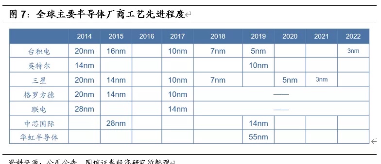
One is the number of nanometers reached in the advanced process. The process reflects the advanced semiconductor manufacturing technology. At present, the most advanced process that can be mass produced is Taiwan Semiconductor Manufacturing Co Ltd's 5nm, and the latest advanced semiconductor foundry in China is Semiconductor Manufacturing International Corporation's 14nm. The 14nm and 5nm here refer to the gate length of the transistor inside the chip, which is generally speaking the minimum linewidth inside the chip. In general, the more advanced the process, the higher the performance of the chip, especially the digital circuit.
The second is to look at the wafer size. 6-inch and 8-inch silicon wafers are mainly used in the production of power semiconductors, 8-inch silicon wafers are used in microcontrollers, and 12-inch silicon wafers are needed for logic chips and memory chips. at present, silicon wafers are developing towards large size with the development of semiconductor technology and the change of market demand.
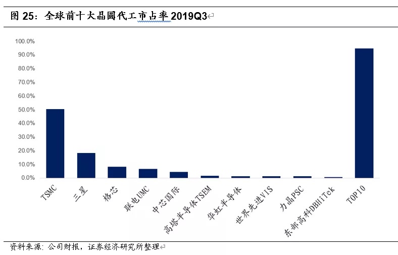
The third is to look at production capacity. In general, semiconductor manufacturers will not easily expand production, production capacity in the short term of about one year is stable, when the semiconductor boom comes, capacity determines the company's income. As of Q3 in 2019, the world's major semiconductor foundry capacity ranking: Taiwan Semiconductor Manufacturing Co Ltd, United Microelectronics Corp, Semiconductor Manufacturing International Corporation, World Advanced, Hua Hong Semiconductor.
The more advanced the process, the better.
First, the cost of upstream IC design is getting higher and higher.
Second, the process approaches the limit, and the mid-stream investment increases but the marginal effect decreases.
Third, customers consider the stability and reliability of the contract factory.
The technical route meets the needs of customers-customers want the investment and development direction of the foundry to be in line with the direction of customer technology development, and the demand for differentiated technology of the existing process.
Expand customer investment value-customers want to get more value from each generation of technology and take full advantage of the significant investment required to design each technology node. Financial soundness ensures supply-customers want the financial soundness of the foundry to meet the demand for chip production over the next decade.
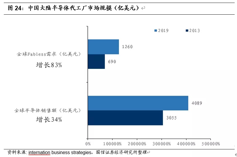
The growth rate of semiconductor foundry is faster than that of semiconductor industry.
Between 2013 and 2019, global semiconductors grew by 34 per cent, while Fabless demand (corresponding to foundry revenues) increased by 83 per cent.
Investment suggestion
We believe that the market has a full understanding of chip design and semiconductor equipment. However, the understanding of semiconductor manufacturing is not enough. At the same time, coupled with the high barriers to semiconductor manufacturing research, the capital market is passive to ignore semiconductor manufacturing.
2020 is the big year of semiconductor manufacturing, we continue to recommend Semiconductor Manufacturing International Corporation and Hua Hong Semiconductor.
Text:
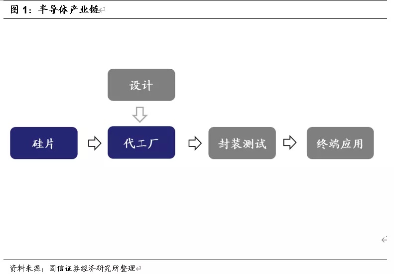
Manufacturing (OEM) is the focus of the semiconductor industry
Semiconductor manufacturing is currently the biggest bottleneck in the development of Chinese mainland Semiconductor. High-end chips, such as computer CPU and mobile phone SOC/ baseband, have been replaced in China. Although there is a gap between performance and international giant products, it can at least be "ready to use".
And semiconductor manufacturing is in the process of "01" breakthrough, if overseas semiconductor foundry does not contract for Chinese mainland design company, then China's semiconductor industry will be seriously affected.
This paper mainly talks about semiconductor manufacturing, which involves silicon and foundry in the semiconductor industry chain.
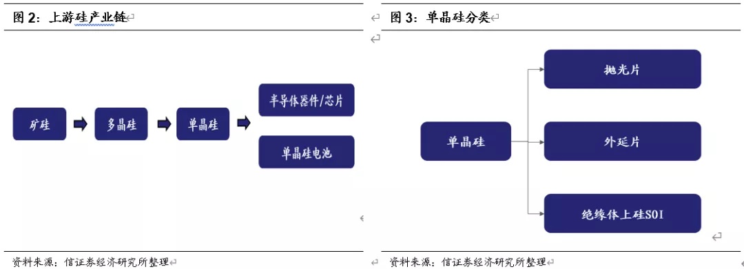
Silicon wafer industry chain
Silicon is a very common element, which widely exists in rock, gravel and dust.
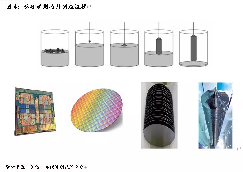
According to the process type, semiconductor wafers can be divided into polished wafers, epitaxial wafers and high-end silicon-based materials represented by SOI wafers.
Generally speaking, polished wafers are used for integrated circuit production lines less than 8 inches, and epitaxial wafers are used for 45nm and 12-inch wafers with line width below. SOI is a new process.
Polished wafer is the most widely used, the largest and the most basic product, and other silicon wafer products are also produced by secondary processing on the basis of polished wafer. The polished wafer removes the residual damage layer on the surface and realizes the flatness of the silicon wafer surface, which can be used to make the substrate materials of memory chips, power devices and epitaxial wafers.
The epitaxial wafer grows a layer of monocrystalline silicon on the polished wafer substrate, which is called the epitaxial layer; the epitaxial layer is injected into the base region, emitter and so on. Because, in bipolar devices and integrated circuits, in order to reduce the collector series resistance, in order to reduce the saturation voltage drop and power consumption. It can be used in the manufacture of general processor chips, graphics processor chips, diodes and IGBT power devices.
SOI silicon wafer can reduce parasitic capacitance and leakage and eliminate latch-up effect. In MOSFET and its integrated circuits, the main purpose is to reduce the turn-on voltage drop and power consumption, sometimes for the need of isolation. In CMOS-IC chips, SOI substrates are more inclined to be used, mainly to reduce or avoid latch-up effect, but also to suppress short channel effect, which is of great significance for ULSI and is used in RF front-end chips, power devices, automotive electronics and other fields.
Silicon on insulator is also used for the control of aerospace electronics, missiles and other weapon systems and new silicon materials for satellite electronic systems. It realizes all-dielectric isolation of CMOS and bipolar circuits, and has the advantages of no latch-up, high speed, low power consumption, high package density, radiation resistance and high temperature resistance (300C).
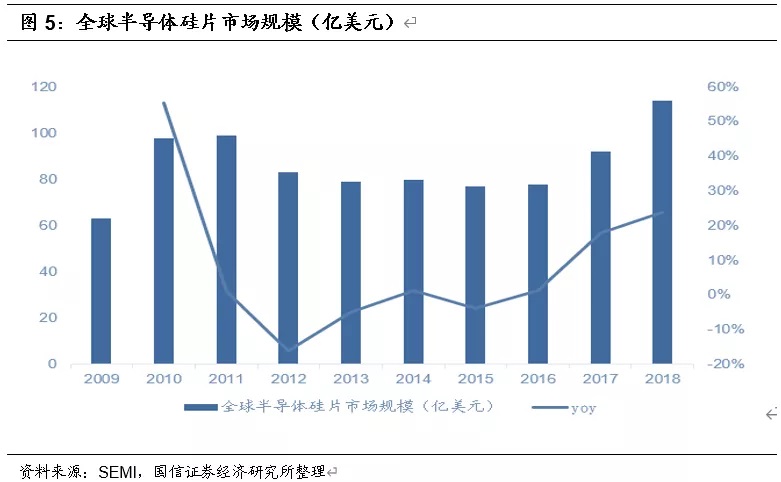
The manufacturing process of silicon wafer is as follows: pulling-slicing-grinding-chamfering-etching-polishing-cleaning-testing, in which crystal drawing, polishing and testing are the core links of silicon wafer manufacturing.
Semiconductor manufacturers carve circuits (semiconductor manufacturing) on qualified silicon wafers and complete them before packaging and testing.
Upstream wafer market scale
The area of global wafer shipments reached 12.73 billion square inches in 2018, an increase of 7.81 per cent over 2017.
Global wafer sales in 2018 were US $11.4 billion (including US $996 million for Chinese mainland semiconductor wafers), an increase of 30.65% over 2017, of which the unit price per square inch was US $0.89, an increase of 21% over 2017.
From 2016 to 2018, the global semiconductor wafer market sales scale CAGR reached 25.75%.
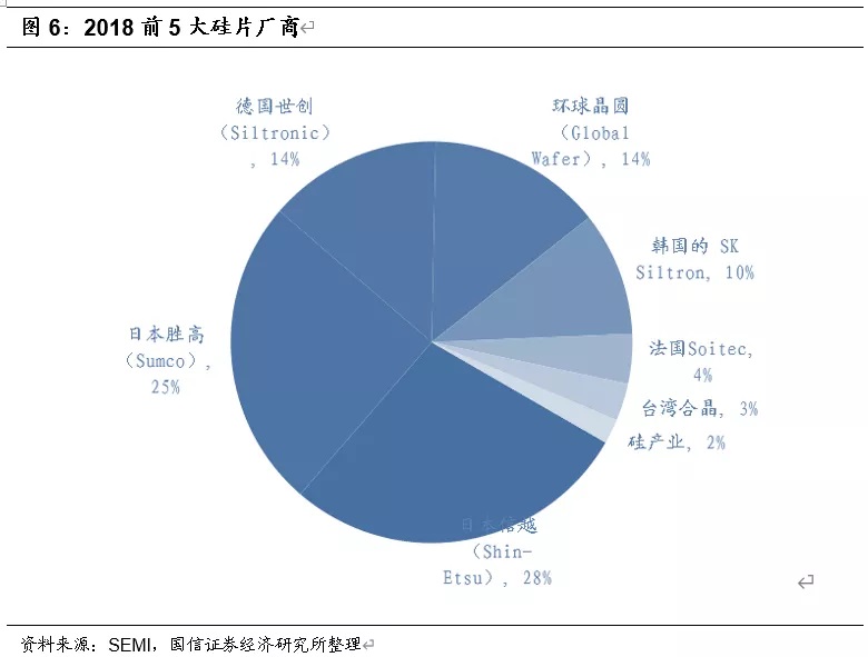
Five major silicon wafer factories monopolize the market
The global semiconductor wafer market is mainly concentrated in several large enterprises with high industry concentration and high technical barriers. The top five wafer manufacturers in 2018 have a combined market share of 95%. The market shares of the top five companies in the industry are: Japan Shinyue Chemical Market share 28%, Japanese SUMCO market share 25%, German Siltronic market share 14%, Taiwan global wafer market share 14%, South Korea SKSiltron market share 11%, French Soitec 4%.
Three indicators of semiconductor foundry
First, how many nanometers does the advanced process reach?
The process reflects the advanced semiconductor manufacturing technology. At present, the most advanced process that can be mass produced is Taiwan Semiconductor Manufacturing Co Ltd's 5nm, and the latest advanced semiconductor foundry in China is Semiconductor Manufacturing International Corporation's 14nm. The 14nm and 5nm here refer to the gate length of the transistor inside the chip, which is generally speaking the minimum linewidth inside the chip.
In general, the more advanced the process, the higher the performance of the chip, especially the digital circuit.
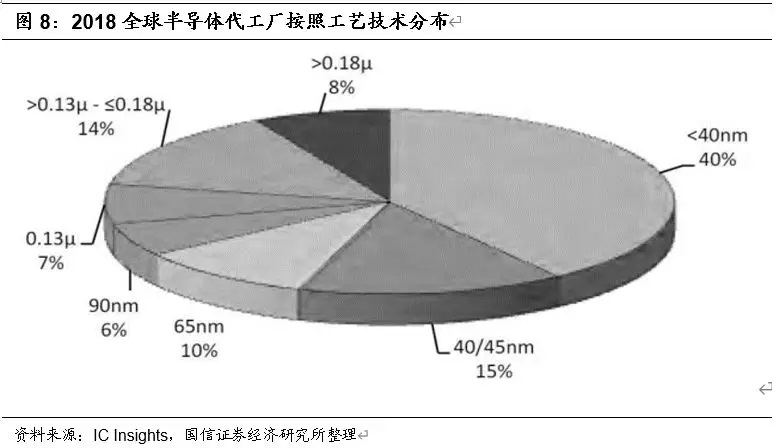
In terms of process composition, 40% of the world's semiconductor foundry revenue comes from advanced process processes of 40nm and below, and this proportion will increase in the future.
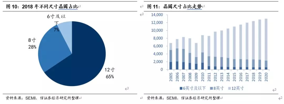
The second is the wafer size.Tend to be large silicon wafers
At present, the main wafer sizes in the world are 6 inches, 8 inches and 12 inches.
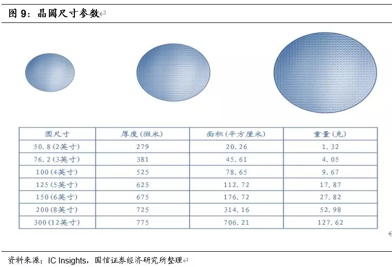
6-inch and 8-inch silicon wafers are mainly used in the production of power semiconductors, 8-inch silicon wafers are used in microcontrollers, and 12-inch silicon wafers are needed for logic chips and memory chips. at present, silicon wafers are developing towards large size with the development of semiconductor technology and the change of market demand.
The average global demand for 12-inch wafers in 2018 will be 6-6.5 million wafers per month, while the average demand for 8-inch wafers will be 550-6 million wafers per month. From a technical point of view, the demand for 12-inch wafers is mainly driven by NAND and DRAM. From a market point of view, the growing storage capacity of smartphones and their dependence on data transmission promote the replacement of solid state hard drives (SSD) with mechanical hard drives (HDD). The use of sensors in smart phones also plays a certain role. 8-inch wafers are more used in the field of automotive electronics, such as the popularity of ADAS systems and in-car entertainment, increasing the market demand for logic circuits and high-precision components, and there is still a huge demand for 8-inch wafers in the long run.
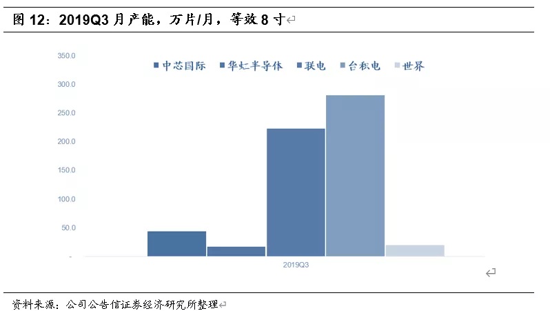
Third, production capacity determines short-term performance.
In general, semiconductor manufacturers will not easily expand production, production capacity in the short term of about one year is stable, when the semiconductor boom comes, capacity determines the company's income.
As of Q3 in 2019, the world's major semiconductor foundry capacity ranking: Taiwan Semiconductor Manufacturing Co Ltd, United Microelectronics Corp, Semiconductor Manufacturing International Corporation, World Advanced, Hua Hong Semiconductor.
The more advanced the process, the better.
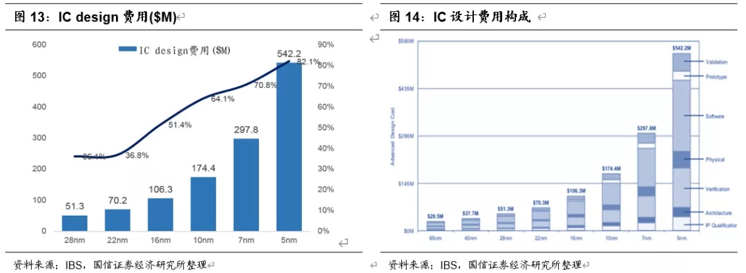
One is upstream IC.The cost of design is getting higher and higher.Advanced process satisfaction provides a good power consumption ratio for equipment, but the cost of IC design is getting higher and higher, and the growth rate of intergenerational design cost is also getting higher and higher. For example, the design cost of the 7nm chip is more than $300m. Huawei mate20 Kirin 980s are manufactured using Taiwan Semiconductor Manufacturing Co Ltd's 7nm process. Kirin 980s are a team of more than 1000 semiconductor engineers that took three years and experienced more than 5000 engineering verifications before they were successfully applied.
IBS estimates that it costs $1.5 billion to develop a NVIDIA GPU based on 3nm. From the perspective of economic benefits of chip design, 7nm is a long-standing node, and the cost of power consumption, performance and area of 5nm/3nm is difficult to reach a balance point, unless there are excess shipments to share the cost.
Second, the process approaches the limit, and the mid-stream investment increases but the marginal effect decreases.
Before 14nm, there was a 50% increase in performance and price in the process of improving every 18 months, but after 14nm, the trend has gradually declined.
For example, when the processor speed doubles, but the user experiences less than twice the speed. User experience is a complete system, processor performance is limited by memory, system software, network and so on.
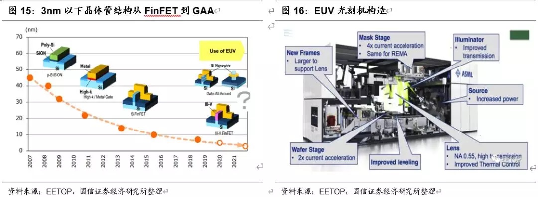
The upgrade of process size requires the cooperation of lithography system, and the lithography system after 7nm has been upgraded from DUV to EUV, and the investment cost has increased sharply. For example, Samsung 7nm production line has invested US $5.6 billion to upgrade the wafer plant of Hwaseong, which needs 8 EUV, each EUV system is 1.5 billion RMB.
In addition, the process upgrade transistor upgrade also needs innovation, 14nm created the FinFET,3nm requires GAA through the transistor structure, transistor-level innovation is a complete transformation of the production line of the foundry.
Third, customers consider the stability and reliability of the contract factory.
The technical route meets the needs of customers-customers want the investment and development direction of the foundry to be in line with the direction of customer technology development, and the demand for differentiated technology of the existing process.
Expand customer investment value-customers want to get more value from each generation of technology and take full advantage of the significant investment required to design each technology node.
Financial soundness ensures supply-customers want the financial soundness of the foundry to meet the demand for chip production over the next decade.
Considering the above factors, Groufonde and United Microelectronics Corp both gave up the development below 14/12nm.
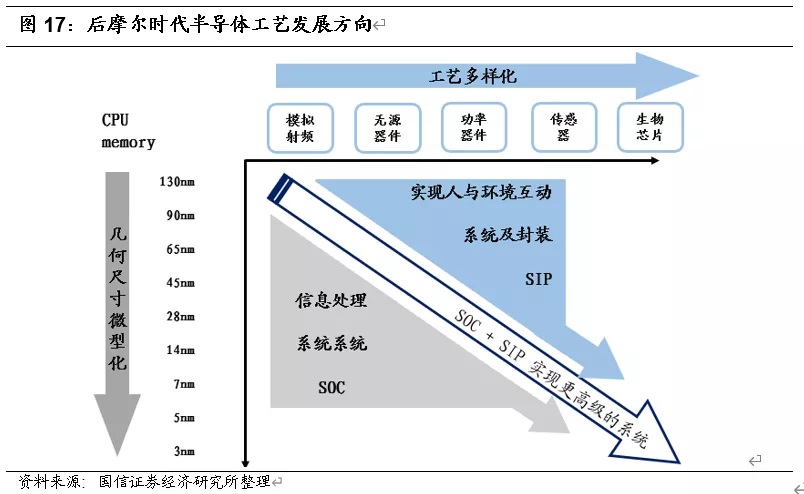
Two-way development of advanced process and special technology
There are two directions for the development of semiconductor technology in the future: one is to continue to pursue advanced process miniaturization, which typically represents Taiwan Semiconductor Manufacturing Co Ltd, Samsung, Intel Corp and Semiconductor Manufacturing International Corporation; the other is to focus on characteristic processes to meet diversified needs and realize the interaction between people and the environment. For example, Hua Hong Semiconductor, United Microelectronics Corp, Groufonde, the world is advanced.
The growth rate of contract manufacturing exceeds that of the semiconductor industry as a whole.
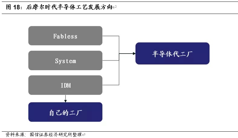
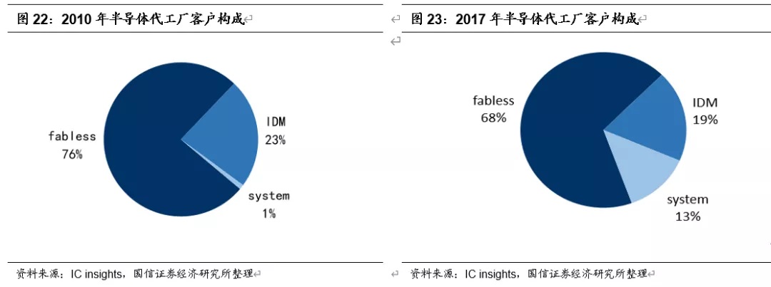
Semiconductor manufacturer mode is divided into Fabless mode with only design and no manufacturing and IDM with design and manufacture. Fabless, IDM and system manufacturers are all customers of contract manufacturers.
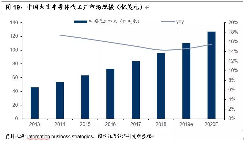
In 2019, the size of Chinese mainland semiconductor contract manufacturing market is expected to grow 14.6% year on year at US $11 billion.
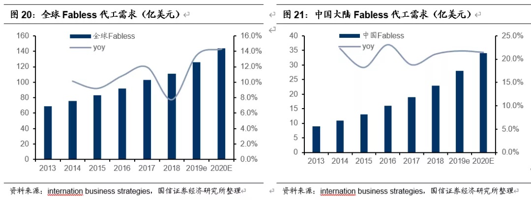
The global demand for contract manufacturing of Fabless semiconductors in 2019 was US $126 billion, an increase of 13.5% over the same period last year, of which the demand in China was US $28 billion, an increase of 21.7% over the same period last year.
DIM manufacturers look for contract factories when their production capacity is insufficient, and some system manufacturers make their own chips, such as Huichuan (frequency converter), Hefei Sunshine (power supply) and Inverter (frequency converter). In order to reduce costs and ensure the supply chain, these terminal system vendors design their own chips to be manufactured by contract manufacturers.
Semiconductor contract manufacturing is growing faster than the semiconductor industry, with global semiconductor growth of 34 per cent from 2013 to 2019, while Fabless demand (corresponding to foundry revenue) increased by 83 per cent.
Global ranking of contract manufacturers
The top ten Q3 fabs in 2019 are: Taiwan Semiconductor Manufacturing Co Ltd, Samsung, Gro Fonder, United Microelectronics Corp, Semiconductor Manufacturing International Corporation, Gao Ta, Huahong, World Advanced, Lijing, and Eastern Hi-Tech.
Semiconductor Manufacturing International Corporation, the leader of domestic contract manufacturing, ranks fifth with a market share of 4.4%.
Investment suggestion
We believe that the market has a full understanding of chip design and semiconductor equipment. However, the understanding of semiconductor manufacturing is not enough. At the same time, coupled with the high barriers to semiconductor industry research, the capital market is passive to ignore semiconductor manufacturing. 2020 is the big year of semiconductor manufacturing, we continue to recommend Semiconductor Manufacturing International Corporation and Hua Hong Semiconductor.
Industry investment risk
First, depreciation in asset-heavy industries affects profits.
Second, capital expenditure is large, which affects cash flow.
Third, the easing of the trade war has led to global competition for domestic contract manufacturers.
Edit / Jeffy