
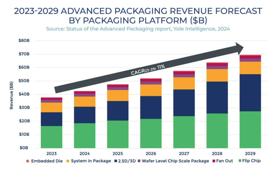
 根据Yole最新发布的《2024年先进封装状况》报告,预计2023-2029年先进封装市场的复合年增长率将达到11%,市场规模将扩大至695亿美元。
When it comes to wafer foundry, Taiwan Semiconductor is definitely the industry's top leader.
When it comes to wafer foundry, Taiwan Semiconductor (TSM.US) is definitely the industry's top leader.
Nowadays, with the slowdown of Moore's Law and the push of the AI wave, advanced packaging as a key technology path to enhance chip performance is being further pushed to the forefront of the semiconductor industry.
 According to the latest report on the status of advanced packaging in 2024 released by Yole, the compound annual growth rate of the advanced packaging market is expected to reach 11% from 2023 to 2029, and the market size will expand to $69.5 billion.
Under the market potential, leading companies in the front and back-end supply chain are actively investing in advanced packaging technology.
In this process, we can clearly observe that traditional assembly and testing (OSAT) companies are gradually falling behind in the market competition. Many companies that originally focused on foundry services are also beginning to enter the advanced packaging market. From Taiwan Semiconductor's CoWoS, to Intel's EMIB, to Samsung's X-Cube, various 2.5D and 3D packaging technologies are emerging one after another and maturing. In this blue ocean of packaging, a hot trend similar to a thousand sails competing is being stirred up.
Taiwan Semiconductor is gradually approaching the top spot in the advanced packaging market.
Recently, research institution ALETHEIA asserts that Taiwan Semiconductor is not only the leader in advanced process technology, but also the advanced packaging is set to take off next year, with the potential to become the largest packaging service provider, a unique presence in the semiconductor industry.
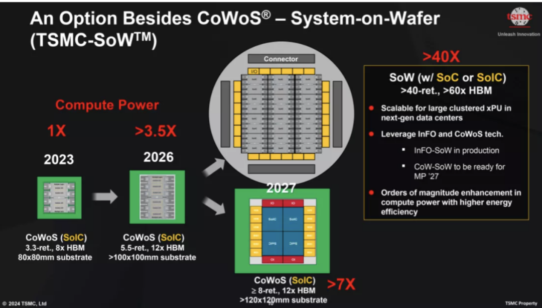
Thanks to the accelerated adoption of Chiplet architecture, driving the progress of 2.5D/3D packaging technology, Taiwan Semiconductor's advanced packaging capacity in 2026 will be ten times that of 2023, and in 2027, it will reach 15 times that of 2023.
It is foreseeable that in the post-Moore era, advanced packaging is attracting attention from capital and industry. Taiwan Semiconductor, as a leader in the field, is actively entering the realm of advanced packaging with exceptional innovation in technology and capacity iteration.
Taiwan Semiconductor Leading the Advanced Packaging Market
Looking back over the development of the past few years, Taiwan Semiconductor has introduced a strategic technological approach supporting advanced packaging, leading the way into a new era of heterogeneous integration.
As early as 2008, Taiwan Semiconductor established the Integrated Interconnect and Packaging Technology Department (IIPD) to enter the field of advanced packaging.
At that time, against the backdrop and impact of the financial crisis, Taiwan Semiconductor faced operational losses, forced pay cuts, and layoffs. Concurrently, in the 28nm process technology segment, research and development costs were rapidly rising; Taiwan Semiconductor also faced strong challenges from Samsung, Intel, GlobalFoundries, and United Microelectronics.
Amid internal and external challenges, Morris Chang returned to take the helm of Taiwan Semiconductor, bringing back the retired Shang-Yi Chiang to lead research and develop advanced packaging technology for differentiation in competition.
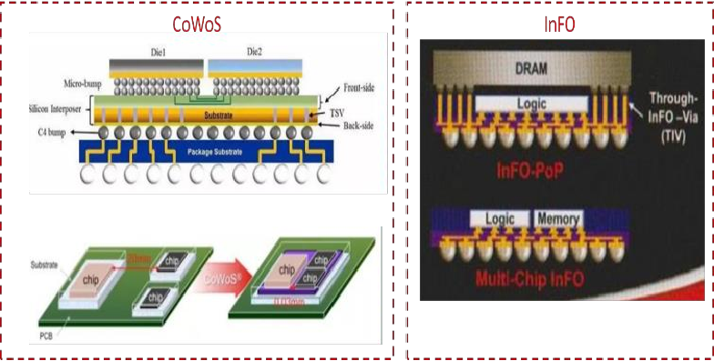
In recent years, Taiwan Semiconductor invests about 10% of its annual capital expenditures in advanced packaging, testing, masks, etc., and has now developed a technology array including 2.5D packaging CoWoS, fan-out packaging InFO, and 3D packaging SoIC.
In the article 'Giant Foundries Compete in Advanced Packaging,' it was mentioned that in 2011, Taiwan Semiconductor introduced its first product - CoWoS, which is one of Taiwan Semiconductor's secret weapons dominating the global advanced packaging sector.
CoWoS (Chip On Wafer On Substrate) is a 2.5D integrated production technology, derived from the combination of CoW and WoS: CoW involves stacking chips on wafers (Chip-on-Wafer), while WoS refers to wafers on substrates (Wafer-on-Substrate), integrated into CoWoS.
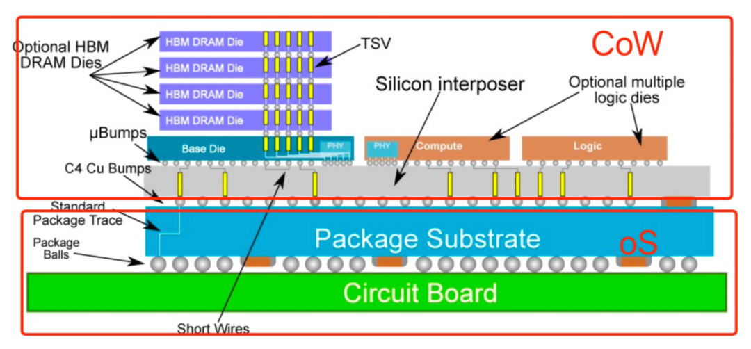
Taiwan Semiconductor's CoWoS structural diagram.
It is reported that this was a concept proposed by Jiang Shangyi in 2006.
The core of CoWoS is to stack different chips in the same silicon interposer to achieve interconnection between multiple chips. In the silicon interposer, Taiwan Semiconductor uses technologies like microbumps (μBmps), through silicon vias (TSVs), etc., replacing traditional wire bonding for interconnections between bare dies, significantly increasing interconnect density and data transmission bandwidth.
CoWoS technology achieves the goals of improving system performance, reducing power consumption, and reducing package size, thereby keeping Taiwan Semiconductor ahead in subsequent packaging technologies. This is also the current popular main packaging technologies such as HBM memory, Chiplet, and others.
According to different intermediaries (interposer), Taiwan Semiconductor's "CoWoS" packaging technology is divided into three types:
CoWoS_S: Using Si substrate as the intermediary layer. This type was the first "CoWoS" technology developed in 2011. In the past, "CoWoS" referred to advanced packaging technology with silicon substrate as the intermediary layer;
CoWoS_R: It uses Redistribution Layer (RDL) as the intermediary layer;
CoWoS_L: It uses Chiplet and RDL as the intermediary layer, combining the advantages of CoWoS-S and InFO technology, with flexible integration.
Taiwan Semiconductor, through early technological accumulation and a large number of successful cases, has iterated its CoWoS packaging technology to the 5th generation.
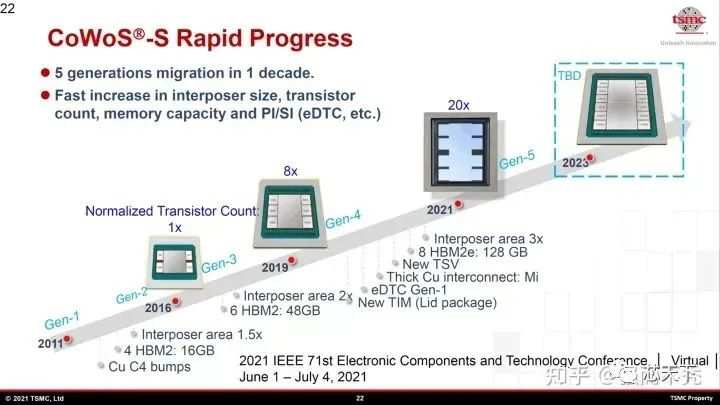
The roadmap of CoWoS packaging technology
However, the now popular CoWoS technology was once in an awkward situation when it was first launched.
Due to its high price, Taiwan Semiconductor's CoWoS packaging only received orders from the FPGA giant Xilinx, which was also the only order received by Taiwan Semiconductor's advanced packaging project team in 2012.
In response, Taiwan Semiconductor decided to take a 'subtraction' approach to CoWoS and developed a cost-effective version of CoWoS technology, namely the InFO technology.
InFO packaging replaces the silicon interposer in CoWoS packaging with polyamide film material, thereby reducing unit cost and packaging height. Both of these are important benchmarks for the success of InFO technology in mobile applications and the HPC market.
Thanks to the introduction of InFO technology, Apple's iPhone 7 and iPhone 7 Plus processors that year adopted InFO packaging technology. This also became a key factor for Taiwan Semiconductor to later monopolize Apple's A-series processor orders.
The product that truly ignited the CoWoS packaging was the AI chip. In 2016, NVIDIA launched the first GPU chip GP100 using CoWoS packaging, kicking off the global AI craze; in 2017, Google and Intel products were successively entrusted to Taiwan Semiconductor for production, using CoWoS packaging.
As a result, the CoWoS technology, which had been on the sidelines for many years due to high costs, ushered in a new situation, with capacity expansion one after another.
In addition, Taiwan Semiconductor also announced innovative system integration single-chip multi-chip 3D stacking technology - SoIC.
SoIC is a new generation of multi-chip stacking technology developed based on taiwan semiconductor's CoWoS and Wafer on Wafer (WoW) packaging technology, these two solutions provide excellent design flexibility when mixing and matching different chip functions, sizes, and technology nodes.
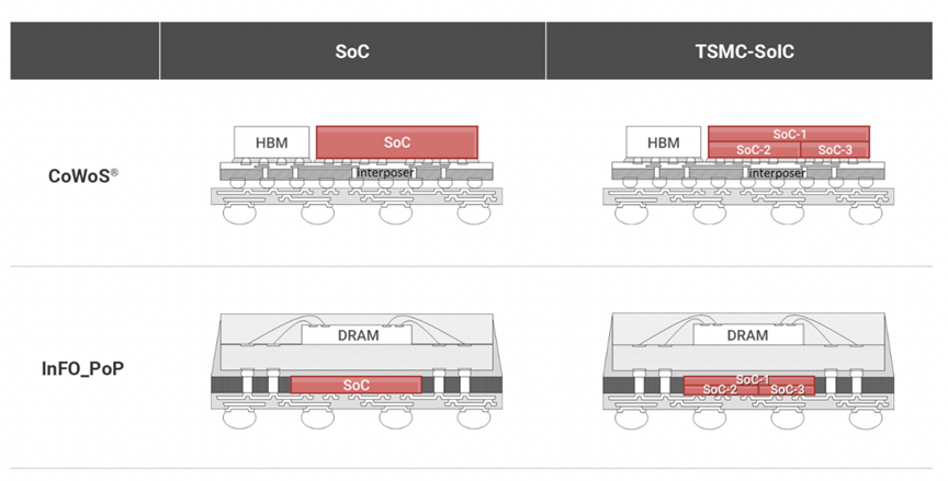
The launch of SoIC also signifies that Taiwan Semiconductor now has the ability to directly produce 3D ICs for customers. Compared to 2.5D packaging solutions, SoIC has higher bump density, faster transmission speed, and lower power consumption.
In 2020, Taiwan Semiconductor announced the merger of its 2.5D and 3D packaging products into a comprehensive brand, 3DFabric, further integrating process technology and packaging technology to enhance competitiveness.
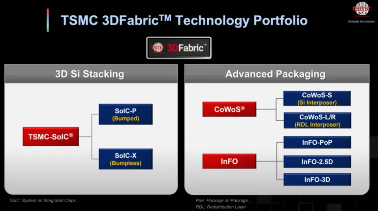
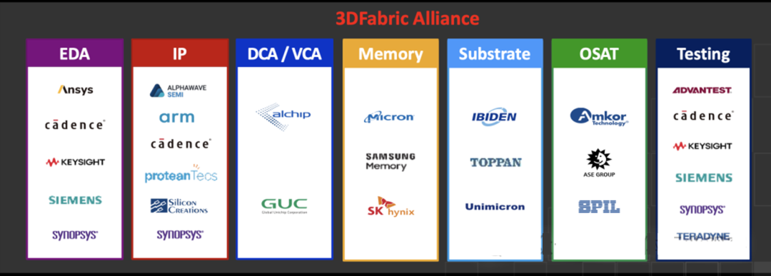
In order for all these packaging technologies to function throughout the entire ecosystem, Taiwan Semiconductor established the 3DFabric Alliance in 2022, collaborating with leading companies in 7 areas including EDA, IP, DCA/VCA, memory, OSAT, substrate, and testing. The aim is to standardize its proprietary packaging technology in order to preemptively capture the dominant position in the future market. The organization also drives the development of tools, processes, IPs, and interoperability of the entire 3D fabric stack.
Taiwan Semiconductor's advanced packaging technology is continuously upgrading.
At a recent North American technical seminar, Taiwan Semiconductor detailed its future roadmap for semiconductor and chip packaging technology.
CoWoS Technology Iteration Trend
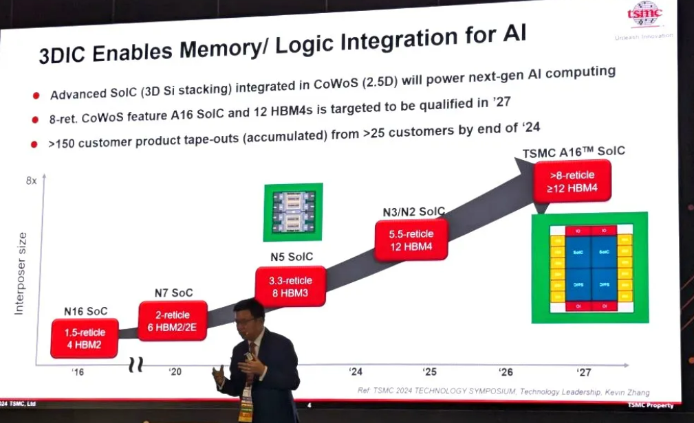
First is the CoWoS packaging technology, the current CoWoS iteration supports an interposer (silicon-based layer) size up to 3.3 times the typical photomask used in lithography. By 2026, TSMC's 'CoWoS_L' is expected to increase its size to approximately 5.5 times the mask size, leaving space for larger logic chips and up to 12 HBM memory stacks. Just a year later in 2027, CoWoS will expand to 8 times the mask size or even larger.
In a recent keynote speech, Hsoung Chun-hung, TSMC's Director of Advanced Packaging Integration, stated that as the best solution that meets all conditions, TSMC's advanced packaging focus will gradually shift from CoWoS-S to CoWoS-L, with CoWoS-L being a key technology in the future blueprint.
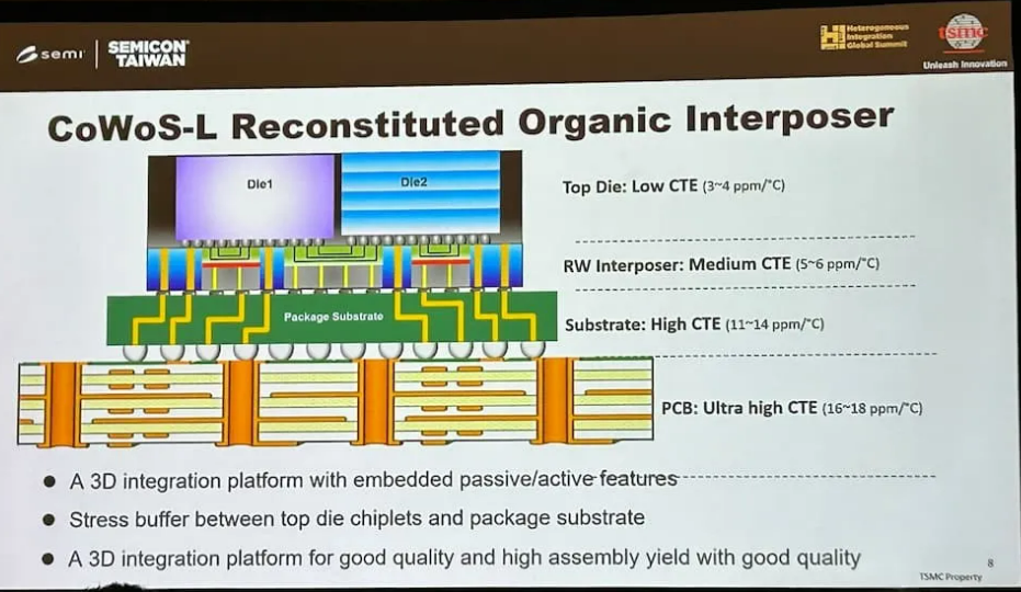
Due to the high cost of Top Die, CoWoS-L is a better solution than CoWoS-R and CoWoS-S in meeting all conditions. Because of its flexibility, it can achieve heterogeneous integration in the interposer layer, with its specialized size and functions. CoWoS-L is compatible with various high-performance top-tier chips, such as advanced logic, SoIC, and HBM.
SoIC Evolution Roadmap
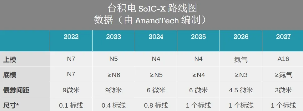
In response to SoIC-X (non-protruding block) packaging technology, taiwan semiconductor expects that by 2027, SoIC-X technology will shrink from the current 9μm protrusion spacing to a 3μm spacing. Combining A16 and N2 chips together, the improved hybrid bonding technology aims to enable taiwan semiconductor's large HPC customers (AMD, broadcom, intel, nvidia, etc.) to build large, ultra-dense modular processor designs for demanding applications, significantly increasing the bandwidth density and product performance of assembled chips.
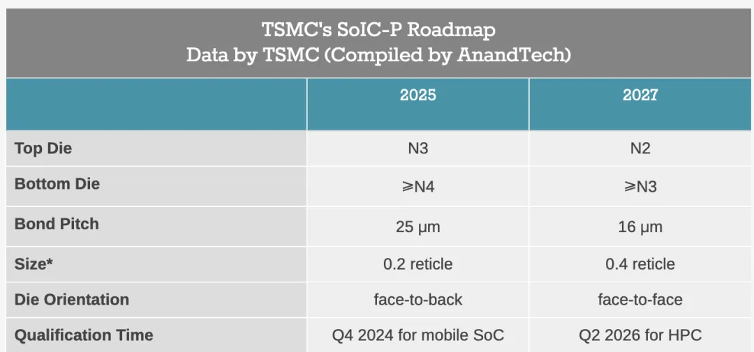
In addition to developing non-protruding block SoIC-X packaging technology for devices requiring ultra-high performance, taiwan semiconductor will soon introduce protruding block SoIC-P packaging technology. SoIC-P is designed for cheaper, lower-performance applications that still require 3D stacking but do not need the additional performance and complexity brought by non-protruding block copper-to-copper TSV connections. This packaging technology will enable a broader range of companies to utilize SoIC. While taiwan semiconductor cannot represent its clients' plans, the cheaper technology version may make it suitable for more cost-conscious consumer applications.
According to taiwan semiconductor's current plans, by 2025, they will offer Front-to-Back (F2B) protruding block SoIC-P technology, which pairs a 0.2 lithography mask size N3 (3 nanometer class) top chip with an N4 (4 nanometer class) bottom chip using 25μm pitch microbumps (µbumps) for connection. In 2027, taiwan semiconductor will introduce Front-to-Front (F2F) protruding block SoIC-P technology, which can place the N2 top chip on the N3 bottom chip with a 16μm spacing.
To make SoIC more popular and easier to obtain among chip developers, there is still a lot of work to be done, including continued improvement of its chip-to-chip interface. However, taiwan semiconductor seems very optimistic about industry adoption of SoIC, expecting to release around 30 SoIC designs by 2026-2027.
taiwan semiconductor emphasizes that 3D IC is a key method of integrating AI chip storage with logic chips. It is estimated that the global semiconductor market will become a trillion-dollar industry by 2030, with HPC and AI being key drivers, accounting for 40%. This also makes AI chips a key driver for 3D IC packaging.
Photonics packaging, Taiwan Semiconductor's next target.
While vigorously developing traditional semiconductor packaging, light has also become a focus of Taiwan Semiconductor.
At this year's technical symposium, Taiwan Semiconductor also revealed the '3D Optical Engine' strategy, aiming to integrate lightning-fast optical interconnects into its customer designs. With the explosive increase in bandwidth demand, copper wires are gradually unable to meet the requirements of cutting-edge data centers and HPC workloads, while utilizing integrated silicon photonics optical links can provide higher throughput and lower power consumption.
It is understood that Taiwan Semiconductor is developing the compact General-Use Photon Engine (COUPE) technology to support the explosive growth in data transmission brought by the AI boom. COUPE uses SoIC-X chip stacking technology to stack electronic chips on top of photonic chips, providing the lowest impedance at the chip interface and higher energy efficiency than traditional stacking methods.
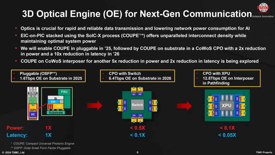
Taiwan Semiconductor plans to certify COUPE as a small pluggable device in 2025, and then integrate it as a Co-Packaged Optics (CPO) in CoWoS packaging in 2026, directly introducing optical connections into the packaging.
From its roadmap, Taiwan Semiconductor's first-generation product inserts into standard optical fiber ports at a speed of 1.6Tbps, twice that of current high-end Ethernet; the second-generation product increases the speed to 6.4Tbps by integrating COUPE with processors into Taiwan Semiconductor's CoWoS packaging; the ultimate result of the roadmap is the CoWoS 'COUPE Intermediate Layer' design, with fiber optic bandwidth reaching an astonishing 12.8Tbps.
Currently, optical components and silicon photonics components are still in the early stages of flourishing, with the consumption of energy becoming an important issue as the AI era demands massive calculations and a large amount of data transmission, leading to the introduction of silicon photonics components as an important trend in data centers.
In addition, Taiwan Semiconductor is also advancing the fan-out panel level packaging (FOPLP) process. A dedicated research and development team and production line have been established. However, it is still in the early stages, and related achievements may be unveiled within 3 years. Wei Zhejia also mentioned that in the future, HPC customers such as NVIDIA and AMD may adopt next-generation advanced packaging technology, using glass substrates instead of existing materials.
Overall, Taiwan Semiconductor is stepping up its efforts to enter the advanced packaging and testing field. One key reason is the desire to extend its advanced manufacturing technology by producing high-end CPU, GPU, and FPGA chips, and providing corresponding packaging and testing processes to offer a complete "manufacturing + testing" solution.
As Taiwan Semiconductor's Chairman and CEO Wei Zhejia proposed the concept of "wafer foundry 2.0," it includes not only traditional wafer manufacturing but also packaging, testing, mask making, and IDM (excluding memory chips). The boundaries of wafer foundry are gradually blurring, expanding the definition. However, Taiwan Semiconductor will focus on the most advanced backend testing technology to help customers manufacture cutting-edge products.
Insufficient supply of advanced packaging capacity, Taiwan Semiconductor accelerates expansion.
With the comprehensive explosion of AI demand, Taiwan Semiconductor's CoWoS capacity has been continuously tight since 2023. Taiwan Semiconductor's President Wei Zhejia stated in July of this year that the demand for CoWoS is "very strong." To address strong customer demand, Taiwan Semiconductor is rapidly expanding its advanced packaging capacity. Taiwan Semiconductor aims to double its capacity in both 2024 and 2025, with the goal of achieving basic supply-demand balance between 2025 and 2026. The company plans to continue to increase investment in the coming years to ensure further expansion of capacity to meet market demand.
The industry expects that by the end of this year, Taiwan Semiconductor's CoWoS monthly capacity could reach 0.045 to 0.05 million pieces, showing a multiple growth from 0.015 million pieces in 2023. By the end of 2025, CoWoS monthly capacity will reach a new peak of 0.05 million pieces.
Currently, Taiwan Semiconductor has a total of five advanced packaging plants located in Hsinchu, Zhongke, Nankang, Longtan, and Zhunan. Among them, the AP6 in Zhunan was officially put into operation in June 2023. It is Taiwan Semiconductor's first fully automated factory that integrates 3D Fabric from the front to the back end processes and testing. After a year of operation, it has become the largest CoWoS packaging base in Taiwan, China.
This expansion plan not only involves doubling the capacity but also the investment and use of multiple new factories. In August 2023, Taiwan Semiconductor spent 17.14 billion New Taiwan dollars to purchase the AUO Nankang 4 factory (AP8 plant area), scheduled to start production in the second half of next year. The factory's future packaging capacity is expected to be 9 times that of Taiwan Semiconductor's advanced packaging plant in Zhunan. The supply chain believes that future production lines for advanced wafer foundry, fan-out packaging, 3D IC, and other processes may be established there. Taiwan Semiconductor's acquisition of AUO Nankang 4 factory this time is mainly to avoid lengthy environmental assessment steps. It is expected that only internal modifications are needed, and it can officially start production next year.
In addition, Taiwan Semiconductor is also constructing 2 CoWoS advanced packaging plants in the Chiayi Science Park. The two planned packaging plants are expected to start mass production in 2028, mainly focusing on System-in-Integrated-Chip (SoIC).
It is worth mentioning that Taiwan Semiconductor is not only expanding production in Taiwan but also seeking suitable factory locations on a global scale, even considering building advanced packaging plants in Japan and the USA.
Recently, there have been reports that Taiwan Semiconductor and chip packaging company Amkor have announced that the two companies have signed a memorandum of understanding to collaborate on chip production, packaging, and testing in Arizona, USA. Taiwan Semiconductor will use these services to support its customers, especially those using Taiwan Semiconductor's advanced wafer manufacturing facility in Phoenix.
Furthermore, Taiwan Semiconductor will continue to cooperate with outsourced OSAT for the layout of advanced packaging to meet customer demands.
At the same time, CoWoS is not the only advanced packaging technology production line that Taiwan Semiconductor hopes to rapidly expand its capacity. The company also has System-in-Integrated-Chip (SoIC) 3D stacking technology, with the adoption rate expected to continuously grow in the coming years. In order to meet the demand for its SoIC packaging method, Taiwan Semiconductor will expand SoIC capacity by 100% compound annual growth rate by the end of 2026.
This capacity plan will jump from around 2,000 wafers per month at the end of 2023 to 4,000-5,000 wafers by the end of 2024, potentially surpassing 8,000 wafers in 2025, and doubling again in 2026. Due to the full capacity commitment, Taiwan Semiconductor's related capacity utilization will maintain a high level.
Currently, Taiwan Semiconductor's SoIC technology has entered the mass production phase at the Hsinchu Plant 6 (AP6). Taiwan Semiconductor also plans to expand the advanced packaging and testing at the Chiayi Plant 7 (AP7) in stages, covering not only CoWoS technology but also SoIC.
Behind the series of these actions, it reflects Taiwan Semiconductor's determination and strategy to actively respond to market demand.
From a market perspective, Taiwan Semiconductor's new moves indicate its importance in the global semiconductor industry chain. With the continuous evolution of technology, competitors such as Samsung, Intel, and others are also increasing their investment in advanced packaging technology. This requires Taiwan Semiconductor to continuously innovate to maintain its leading position in the market. Through the layout of new factories, Taiwan Semiconductor can quickly increase market share, especially in the current trend of surging demand for high-performance chips.
Taiwan Semiconductor's two "swords"
After the Moore era, advanced packaging is valued, and chip packaging testing is becoming increasingly important as the semiconductor industry develops.
Yole emphasizes that the advanced packaging supply chain is undergoing significant transformation. OSATs are expanding their testing capabilities, while pure testing companies are investing in packaging and assembly. Foundries are entering the packaging field, posing a competitive threat to traditional OSATs. Participants from different backgrounds are entering the market.
Companies with different business models are competing in the same high-end packaging market space. However, manufacturers in different formats have varying resource allocations and differences in technological development routes in the packaging business.
For foundries, due to the continuity of the front-end processes involved in 2.5D/3D packaging technology, wafer foundries have a deep understanding of the front-end processes and a more profound understanding of the overall wiring architecture, following a route of highly integrated chip manufacturing and packaging. Therefore, in high-density advanced packaging, Foundries have more advantages than traditional OSATs.
Looking back at Taiwan Semiconductor's rapid layout and goals, Taiwan Semiconductor's integrated business model, combined with front-end manufacturing and advanced packaging capabilities, is becoming the industry benchmark and will directly impact the future market landscape.
ALETHEIA estimates that Taiwan Semiconductor's revenue from the packaging business in 2026 will reach an astonishing $25 billion, not only growing 3.5 to 4 times compared to 2023, surpassing the sum of all mature processes, and being on par with the 4 and 5-nanometer process scale. By then, it will contribute nearly 20% of the annual revenue. If further considering Taiwan Semiconductor's price increase for advanced processes and CoWoS, Taiwan Semiconductor's revenue in 2026 could reach $140 billion, double that of 2023, with the profit part nearly 2.5 times that of 2023.
Looking at the semiconductor wafer foundry industry, there is currently no sign of AI slowing down, on the contrary, under the momentum of 2/3/5 nanometer process and CoWoS expansion, the outlook for Taiwan Semiconductor remains optimistic.
As stated at the beginning of the article: "Taiwan Semiconductor is not only the leader in advanced processes, but also the advanced packaging is set to take off next year, poised to become the largest packaging service provider, making it a unique presence in the semiconductor industry."
This article is reproduced from "Observations in the semiconductor industry"; edited by Finance and Economics Intelligence Editor: Li Fo.
