
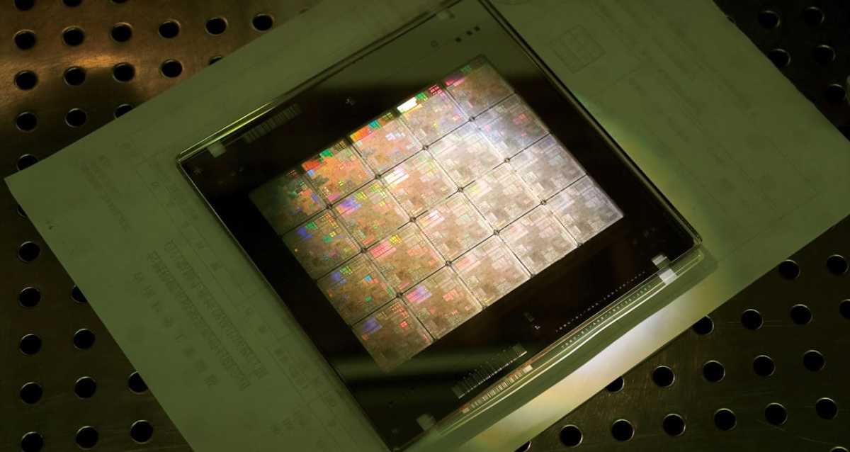
 计算光刻是电脑芯片制造的关键步骤。ASML对它的定义是,利用计算机建模、仿真和数据分析等手段,预测、校正、优化和验证光刻工艺在一系列图案、工艺和系统条件下的成像性能。它涉及电磁物理、光化学、计算几何、迭代优化和分布式计算这些复杂的计算,是整个半导体设计和制造过程中计算最密集的工作负载。晶圆代工厂通常会专门为这些计算设立大型数据中心。而现在先进芯片的尺寸越来越小,降至3nm及以下,需要计算光刻更加精准,计算光刻所需的时间也越来越多。没有更强大的计算光刻很难实现复杂的掩模版设计。计算光刻历来是将新技术节点和电脑架构推向市场的瓶颈。
Nvidia's platform cuLitho has significantly increased the speed of the crucial step of computing lithography in chip manufacturing. Through this platform, Nvidia and Taiwan Semiconductor have respectively increased the speed of the curve process of optical masks and the traditional Manhattan-style process by 45 times and nearly 60 times. Building on the accelerated process speed of cuLitho, Nvidia's developed generative AI application algorithm further doubles the speed.
During the "NVIDIA AI Summit" held in Washington on Tuesday, October 8th, NVIDIA emphasized the achievements of its collaboration with Taiwan Semiconductor in accelerating computing: NVIDIA's computing lithography platform, cuLitho, is now in production at Taiwan Semiconductor, further significantly increasing the speed of this foundational step in chip manufacturing and reducing energy consumption.
NVIDIA stated that cuLitho is introducing accelerated computing into the computing lithography field. Putting cuLitho into production enables Taiwan Semiconductor to expedite the development of next-generation chip technologies, as the current production process is approaching the physical limits. Applying cuLitho in production at Taiwan Semiconductor can enhance the speed of manufacturing next-generation advanced semiconductor chips and surpass physical limitations.
 Computing lithography is a crucial step in computer chip manufacturing. ASML defines it as using computer modeling, simulation, data analysis, and other methods to predict, correct, optimize, and validate imaging performance of lithography processes under various patterns, processes, and system conditions. It involves complex calculations in electromagnetic physics, photochemistry, computational geometry, iterative optimization, and distributed computing, making it the most computationally intensive workload in the entire semiconductor design and manufacturing process. Wafer fabs typically establish large data centers specifically for these computations. As advanced chips shrink in size to 3nm and below, the need for precise computing lithography increases, and the time required for computing lithography grows. Achieving complex mask designs without more powerful computing lithography is challenging. Computing lithography has historically been the bottleneck in bringing new technology nodes and computer architectures to the market.
At last year's NVIDIA developer conference GTC, NVIDIA introduced the cuLitho computing lithography technology software library based on GPUs, described as a game-changing software in the computing lithography field. The core of cuLitho consists of a set of parallel algorithms invented by NVIDIA scientists, enabling all parts of the lithography process to run in parallel. What previously required 0.04 million CPU systems can now be done with just 500 NVIDIA DGX H100 systems. Wafer fabs using cuLitho can increase their mask lithography output by 3-5 times per day while reducing power consumption by 9 times compared to current configurations.
This Tuesday, NVIDIA reiterated the achievements disclosed at this year's GTC conference. Each year, advanced fabs consume hundreds of billions of hours of CPU computing time for computing lithography. One chip mask set typically requires 30 million hours or more of CPU computing time, necessitating large data centers for fabs. Accelerated computing has enabled 350 sets of NVIDIA H100 Tensor Core GPU systems to replace 0.04 million CPU systems, speeding up production, while reducing costs, space requirements, and power consumption.
TSMC CEO C.C. Wei stated at this year's NVIDIA GTC conference that by integrating GPU-accelerated computing into TSMC's workflow with NVIDIA, TSMC significantly improves performance, increases throughput, shortens cycle times, and reduces power consumption.
At this year's GTC conference, nvidia disclosed that since its launch last year, cuLitho has brought new opportunities for taiwan semiconductor's innovative patterning technology. cuLitho tests conducted on a shared workflow show that nvidia and taiwan semiconductor have jointly increased the speed of curved processes and traditional Manhattan processes by 45 times and nearly 60 times, respectively. The difference between these two processes is that the optical mask shape of the curved process is curved, while the optical mask shape of the Manhattan process is limited to horizontal or vertical.
nvidia also mentioned this Tuesday the generative AI application algorithm it developed. It turns out that this algorithm has enhanced the value of the cuLitho platform. On the basis of speeding up the cuLitho process, the new generative AI workflow has further doubled the speed. Applying generative AI can create nearly perfect inverse optical masks or reverse solutions, addressing the diffraction issues of light in computational lithography, and then deriving the final optical mask through traditional rigorous physical methods, thereby accelerating the entire optical proximity correction (OPC) process by two times.
OPC has been used in semiconductor lithography for thirty years. nvidia stated that in the past thirty years, few technologies like accelerated computing and AI have brought such rapid transformation to OPC. These technologies make physical simulations more accurate and achieve mathematical techniques that were once resource-intensive.
Many changes in wafer fab processes currently require modifications to OPC, increasing computational load and creating bottlenecks in wafer fab development cycles. The greatly improved speed of computational lithography technology accelerates the creation speed of each mask in wafer fabs, thereby shortening the total cycle of developing new technology nodes. More importantly, it enables new computations that were previously impossible.
nvidia gave an example that reverse lithography technology was proposed in scientific literature twenty years ago, but due to long calculation times, accurate calculations on a full chip scale were largely unachievable. With cuLitho, this is no longer the case. Leading foundries will use it to enhance reverse and curved solutions, which will help create the next generation of powerful semiconductors.
Editor/Lambor