为了践行这个目标,台积电封装正在疯狂扩产。
Source: Semiconductor Industry Watch. At yesterday's Conputex conference, Dr. Lisa Su released the latest roadmap. Afterwards, foreign media morethanmoore released the content of Lisa Su's post-conference interview, which we have translated and summarized as follows: Q: How does AI help you personally in your work? A: AI affects everyone's life. Personally, I am a loyal user of GPT and Co-Pilot. I am very interested in the AI used internally by AMD. We often talk about customer AI, but we also prioritize AI because it can make our company better. For example, making better and faster chips, we hope to integrate AI into the development process, as well as marketing, sales, human resources and all other fields. AI will be ubiquitous. Q: NVIDIA has explicitly stated to investors that it plans to shorten the development cycle to once a year, and now AMD also plans to do so. How and why do you do this? A: This is what we see in the market. AI is our company's top priority. We fully utilize the development capabilities of the entire company and increase investment. There are new changes every year, as the market needs updated products and more features. The product portfolio can solve various workloads. Not all customers will use all products, but there will be a new trend every year, and it will be the most competitive. This involves investment, ensuring that hardware/software systems are part of it, and we are committed to making it (AI) our biggest strategic opportunity. Q: The number of TOPs in PC World - Strix Point (Ryzen AI 300) has increased significantly. TOPs cost money. How do you compare TOPs to CPU/GPU? A: Nothing is free! Especially in designs where power and cost are limited. What we see is that AI will be ubiquitous. Currently, CoPilot+ PC and Strix have more than 50 TOPs and will start at the top of the stack. But it (AI) will run through our entire product stack. At the high-end, we will expand TOPs because we believe that the more local TOPs, the stronger the AIPC function, and putting it on the chip will increase its value and help unload part of the computing from the cloud. Q: Last week, you said that AMD will produce 3nm chips using GAA. Samsung foundry is the only one that produces 3nm GAA. Will AMD choose Samsung foundry for this? A: Refer to last week's keynote address at imec. What we talked about is that AMD will always use the most advanced technology. We will use 3nm. We will use 2nm. We did not mention the supplier of 3nm or GAA. Our cooperation with TSMC is currently very strong-we talked about the 3nm products we are currently developing. Q: Regarding sustainability issues. AI means more power consumption. As a chip supplier, is it possible to optimize the power consumption of devices that use AI? A: For everything we do, especially for AI, energy efficiency is as important as performance. We are studying how to improve energy efficiency in every generation of products in the future-we have said that we will improve energy efficiency by 30 times between 2020 and 2025, and we are expected to exceed this goal. Our current goal is to increase energy efficiency by 100 times in the next 4-5 years. So yes, we can focus on energy efficiency, and we must focus on energy efficiency because it will become a limiting factor for future computing. Q: We had CPUs before, then GPUs, now we have NPUs. First, how do you see the scalability of NPUs? Second, what is the next big chip? Neuromorphic chip? A: You need the right engine for each workload. CPUs are very suitable for traditional workloads. GPUs are very suitable for gaming and graphics tasks. NPUs help achieve AI-specific acceleration. As we move forward and research specific new acceleration technologies, we will see some of these technologies evolve-but ultimately it is driven by applications. Q: You initially broke Intel's status quo by increasing the number of cores. But the number of cores of your generations of products (in the consumer aspect) has reached its peak. Is this enough for consumers and the gaming market? Or should we expect an increase in the number of cores in the future? A: I think our strategy is to continuously improve performance. Especially for games, game software developers do not always use all cores. We have no reason not to adopt more than 16 cores. The key is that our development speed allows software developers to and can actually utilize these cores. Q: Regarding desktops, do you think more efficient NPU accelerators are needed? A: We see that NPUs have an impact on desktops. We have been evaluating product segments that can use this function. You will see desktop products with NPUs in the future to expand our product portfolio.
To meet the capacity demands for advanced packaging of AI servers, Taiwan Semiconductor is gearing up.
At the financial report meeting in July, $Taiwan Semiconductor (TSM.US)$ Chairman Wei Zhejia also mentioned in response to analysts at the conference about the tight CoWoS capacity related to advanced packaging. The hot demand for artificial intelligence has driven the demand for CoWoS, and Taiwan Semiconductor's CoWoS demand is very strong. Taiwan Semiconductor continues to expand and hopes to achieve supply-demand balance by 2025-2026. The capital expenditure for CoWoS cannot be clearly stated at present because efforts are made every year to increase capacity. As mentioned before, this year's capacity has more than doubled, and the company is working very hard to expand its capacity.
 In order to achieve this goal, Taiwan Semiconductor's packaging is expanding like crazy.

Buying factories, building factories, Taiwan Semiconductor's expansion never stops.
On the expansion route of Taiwan Semiconductor's packaging, the earlier purchase of the 4th factory of Quanta South Korea, with the factory codenamed AP8 Plant Area, is considered a wise choice for the company's packaging development. Through this deal, the company will be able to avoid the years-long environmental assessment phase, and it is expected to start production at this factory in the second half of next year. According to **** media reports, the future capacity of this factory will be 9 times larger than that of the Zhunan Advanced Packaging Plant, and it will also be involved in wafer foundry and 3D IC.
In mid-August this year, Taiwan Semiconductor announced an investment of 17.14 billion New Taiwan dollars to purchase the 5.5th generation LCD panel factory located in South Science Park from Chimei, which was originally favored by the memory giant Micron until Taiwan Semiconductor and Chimei's joint announcement of the factory transaction information, revealing that Taiwan Semiconductor was one step ahead.
Supply chain sources revealed that the main reason Taiwan Semiconductor will acquire Chimei's Nanke Plant 4 is to bypass the annual environmental assessment steps. Unlike the advanced packaging factory in Chiayi, only internal renovation work is required. The production can start less than a year after the equipment is installed.
Equipment manufacturers pointed out that after the confirmation of the factory transaction, Taiwan Semiconductor initiated plans to build a factory for the AP8 Plant, aiming for production by the second half of 2025. The relevant equipment manufacturing orders will proceed simultaneously, with an expected delivery of machines starting in April next year, about a quarter of trial production, and it should not be difficult to start production in the second half of the year.
Due to the AP8 Plant being nine times larger than the Hsinchu advanced packaging factory, the supply chain believes that not only the CoWoS capacity of advanced packaging, but also future advanced process wafer foundry, fan-out packaging, and 3D IC production lines are likely to be stationed here.
In addition to acquiring factories, Taiwan Semiconductor's previous factory construction is also steadily progressing.
In May of this year, Taiwan Semiconductor's CoWoS advanced packaging factory in Chiayi Science Park began construction, but during the construction process, suspected relics were unearthed. According to cultural heritage laws, the related clearance work is expected to be completed by October of this year, and the progress of Taiwan Semiconductor's Jiake advanced packaging factory is not affected. Taiwan has stated that the planned installation of equipment for the Jiake advanced packaging factory for the third quarter of next year will proceed as scheduled.
According to previous plans, Taiwan Semiconductor will establish two CoWoS advanced packaging factories in Chiayi, originally scheduled for mass production by 2028. In terms of technology, the factory mainly focuses on System Integration on a Chip (SoIC), and Taiwan Semiconductor is also bullish on 3D packaging. Currently, clients include the chip giant AMD. $Advanced Micro Devices (AMD.US)$ Apart from MI300, customers are expected to further enhance by 2026.
Due to the strong demand for CoWoS, Taiwan Semiconductor is still looking for a suitable expansion site across Taiwan. The previous plan for the Copper Gong plant faced soil and water-related issues, while the first plant in Chiayi is temporarily on hold (due to the discovery of a historical site), focusing on the long-term huge demand, driving Taiwan Semiconductor to proactively seek more suitable locations. According to earlier media reports, Chang Li-shan, the Magistrate of Yunlin County, mentioned that the county government has independently initiated the "Huwei Industrial Park Plan" in its close vicinity to the Science Park, Huwei, with an area of approximately 29.75 hectares, to make every effort to attract Taiwan Semiconductor to establish a plant there.
However, recent news suggests that Taiwan Semiconductor has decided to abandon Yunlin and relocate to Pingtung, aside from the land purchased around South Science Park. Taiwan Semiconductor stated that the selection of plant location involves many factors considerations, and they do not rule out any possibilities. Earlier this year, there were even rumors that the leading wafer foundry company, Taiwan Semiconductor, is considering establishing an advanced packaging plant in Japan, illustrating the popularity of this packaging technology.
According to American institutional investors' estimates, Taiwan Semiconductor's CoWoS monthly capacity may exceed 0.032 million units by the end of the year, with the possibility of reaching close to 0.04 million units with the help of partner manufacturers. By the end of 2025, monthly production capacity is expected to be around 0.07 million units.
During the semiconductor exhibition, He Jun, the Vice President of Operations, Advanced Packaging Technology, and Services at Taiwan Semiconductor, revealed that the expected Compound Annual Growth Rate (CAGR) of CoWoS advanced packaging capacity from 2022 to 2026 will exceed 50%, and production expansion will continue until 2026. Previously, it used to take 3 to 5 years to build a plant, but now it has been shortened to within 2 years to meet customer demand.
DIGITIMES Research Center's 'AI Chip Special Report' published in mid-August pointed out that the growth momentum of advanced packaging surpasses that of advanced processes. In the field of advanced packaging, AI chips highly depend on Taiwan Semiconductor's CoWoS packaging technology. As a result, Taiwan Semiconductor's CoWoS capacity expansion CAGR from 2023 to 2028 will exceed 50%, while the annual compound growth rate expansion of wafer foundries in 5nm and below advanced processes from 2023 to 2028 will reach 23%.
While significantly increasing production capacity, Taiwan Semiconductor is also iterating the company's packaging technology to provide more support to customers.
The continuous upgrade of packaging technology.
在最近为北美客户举办的研讨会上,这家芯片制造商公布了芯片封装和尖端光学互连技术的雄心勃勃的路线图。这些进步可能会在未来几年掀起计算性能的浪潮。
首先是芯片封装技术,台积电将其命名为“CoWoS”(晶圆基板上的芯片),它本质上是典型小芯片设计的增强版,其中多个较小的芯片集成到一个封装中。但台积电正在将其提升到令人难以置信的规模和复杂性的新水平。
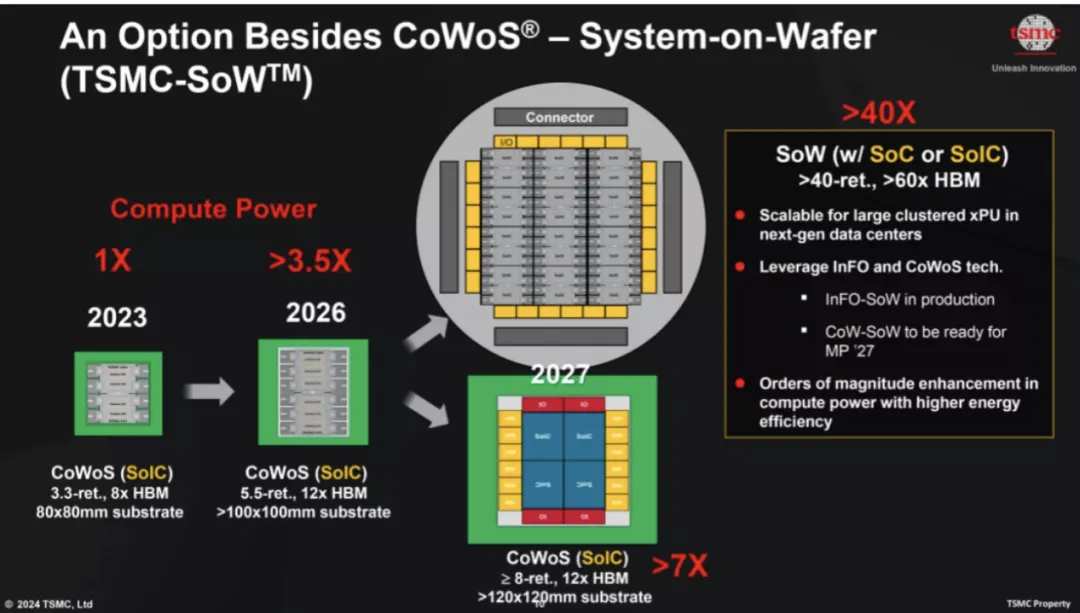
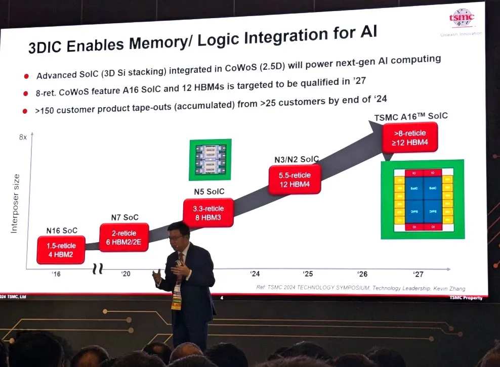
当前的 CoWoS 迭代支持中介层(硅基层)的尺寸高达光刻中使用的典型光掩模的 3.3 倍。但到 2026 年,台积电的“CoWoS_L”将使其尺寸增加到大约 5.5 倍的掩模尺寸,为更大的逻辑芯片和多达 12 个 HBM 内存堆栈留出空间。而仅仅一年后的 2027 年,CoWoS 将扩展到令人瞠目结舌的 8 倍掩模版尺寸甚至更大。
我们谈论的是集成封装,面积达 6,864 平方毫米,比一张信用卡大得多。这些 CoWoS 庞然大物可以整合四个堆叠逻辑芯片以及十几个 HBM4 内存堆栈和额外的 I/O 芯片。
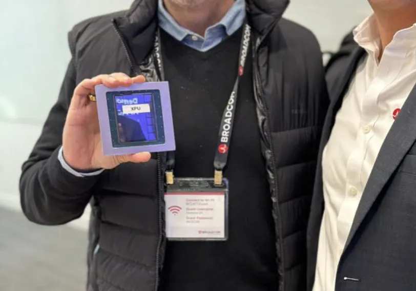
为了让您了解其规模,$Broadcom (AVGO.US)$同时还展示了一款定制的 AI 处理器,该处理器具有两个逻辑芯片和 12 个内存堆栈。该芯片看起来比$NVIDIA (NVDA.US)$ The latest powerful accelerator needs to be larger. According to reports, the chip using the CoWoS packaging technology with Tai Chi Dan wafer substrate (CoWoS) has a computing chip close to the photomask limit (858 square millimeters, 26mm x 33mm).
But compared to the chip TSMC is preparing for 2027, this chip is still insignificant. As mentioned above, TSMC expects its solution to use substrates up to 120x120 millimeters.
In TSMC's packaging roadmap, 3D IC undoubtedly plays an important role.
Also at this year's technical symposium, TSMC outlined a roadmap that by 2027, the technology will shrink from the current 9μm bump pitch to a 3μm pitch, stacking A16 and N2 chips together.
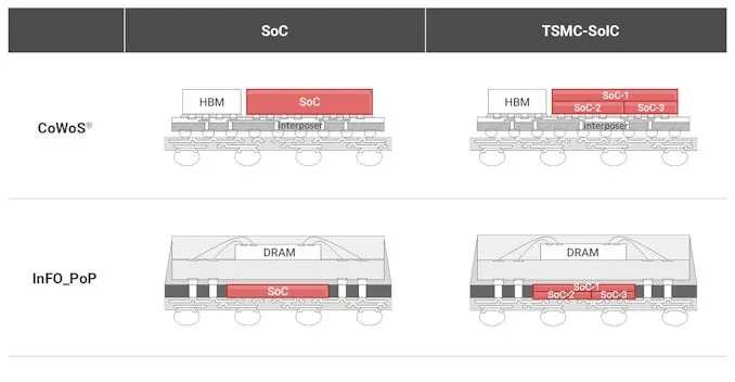
According to reports, TSMC's 3D stacked integrated chip system (SoIC) technology is TSMC's realization of hybrid wafer bonding. Hybrid bonding allows two advanced logic devices to be directly stacked together, achieving ultra-dense (and ultra-short) connections between the two chips, primarily targeting high-performance components. Currently, SoIC-X (no bumps) is used for specific applications, such as AMD's CPU 3D V cache technology, and their Instinct MI300 series AI products. While adoption is growing, the current generation of this technology is limited by chip size and interconnect pitch.
But if everything goes according to TSMC's plan, these limitations are expected to disappear soon. SoIC-X technology will rapidly evolve, and by 2027, it will be possible to assemble a chip pairing the top chip manufactured on TSMC's cutting-edge A16 (1.6 nanometer level) with a bottom chip made using TSMC's N2 (2 nanometer level), with 3μm bond pitch through silicon vias (TSV), three times the density of today's 9μm pitch. Such small interconnects will allow for a significantly higher number of connections overall, greatly increasing the assembly chip's bandwidth density (thereby improving performance).
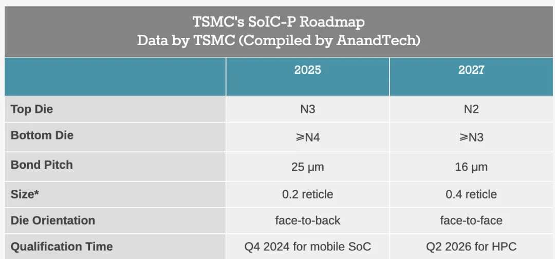
In addition to developing bumpless SoIC-X packaging technology for devices requiring extremely high performance, TSMC will also introduce bump SoIC-P packaging process in the near future. SoIC-P is designed for cheaper low-performance applications that still require 3D stacking but do not need the additional performance and complexity brought by bumpless copper-to-copper TSV connections. This packaging technology will enable a wider range of companies to utilize SoIC, although TSMC cannot speak for its customers' plans, the cheaper technical version may make it suitable for more cost-conscious consumer applications.
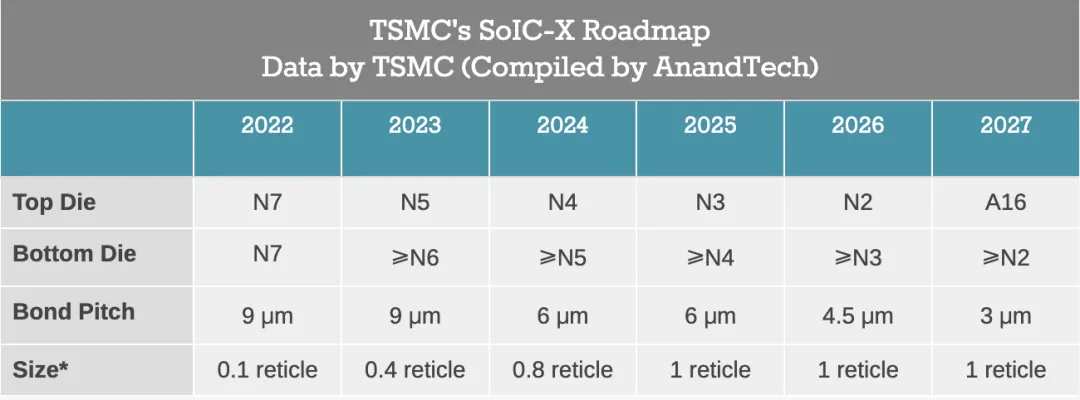
According to TSMC's current plans, by 2025, the company will offer Front2Back (F2B) bump SoIC-P technology, which will pair N3 (3 nanometer level) top chip with N4 (4 nanometer level) bottom chip at 0.2 photomask sizes, using 25μm bump pitch connections. In 2027, TSMC will introduce Front2Front (F2F) bump SoIC-P technology, which will place the N2 top chip on the N3 bottom chip with a 16μm pitch.
To make SoIC more popular and easier to obtain among chip developers, there is still a lot of work to be done, including continuing to improve its chip-to-chip interface. However, Taiwan Semiconductor seems very optimistic about SoIC being adopted by the industry, expecting to release around 30 SoIC designs by 2026 to 2027.
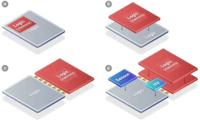
According to reports citing He Jun, Vice President of Advanced Packaging Technology and Services at Taiwan Semiconductor, in a previous speech at semicon Taiwan, Taiwan Semiconductor believes that 3D IC is a key method for integrating AI chip memory with logic chips. He Jun also pointed out that by 2030, the global semiconductor market is estimated to become a trillion-dollar industry, with HPC and AI as key drivers, accounting for 40%, making AI chips a key driver for 3D IC packaging.
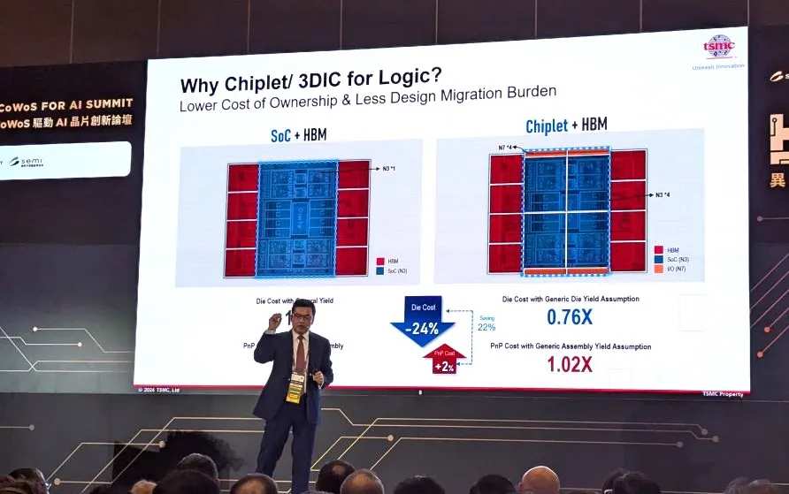
He Jun stated that the reason customers choose to use the 3D IC platform for multi-chip design and manufacturing of AI chips is due to its lower cost and reduced design conversion burden.
He Jun explained that by transitioning traditional SoC+HBM designs to chiplet and HBM architecture, the new logic chip will be the only component that needs to be designed from scratch, while other components like I/O and SoC can use existing process technologies. This method can reduce production costs by up to 76%. He pointed out that although the new architecture may increase production costs by 2%, the overall total cost of ownership (TCO) has increased by 22% due to these efficiency improvements.
However, 3D IC still faces challenges, especially in terms of power efficiency. He Jun emphasized that the key to increasing 3D IC capacity lies in chip size and process complexity. As for chip size, larger chips can accommodate more chips, thereby improving performance. However, this also increases process complexity, with difficulty potentially tripling. In addition, there are risks associated with chip misalignment, damage, and failures during the extraction process.
To address these risk challenges, He Jun identified three key factors: tool automation and standardization, process control and quality, and support for the 3DFabric manufacturing platform.
For tool automation and standardization, the differentiation capabilities of Taiwan Semiconductor with its tool suppliers are crucial. Currently, Taiwan Semiconductor has 64 suppliers and has the capability to lead the way in advanced packaging tools. In terms of process control and quality, Taiwan Semiconductor utilizes high-resolution PnP tools and AI-driven quality control to ensure comprehensive and robust quality management, finally integrating 1,500 materials within the 3DFabric manufacturing platform to optimize the supply chain.
Photonics packaging, Taiwan Semiconductor's next target.
While vigorously developing traditional semiconductor packaging, light has also become a focus of Taiwan Semiconductor.
At this year's technical symposium, Taiwan Semiconductor also revealed its '3D Optical Engine' strategy, aiming to integrate lightning-fast optical interconnects into its customer designs. With the surge in bandwidth demand, copper wires are simply unable to meet the needs of cutting-edge data centers and HPC workloads. The use of integrated silicon photonics optical links can provide higher throughput and lower power consumption.
Taiwan Semiconductor stated that the company is developing the Compact Universal Photonic Engine (COUPE) technology to support the explosive growth in data transmission brought about by the AI boom. COUPE uses SoIC-X chip stacking technology to stack electronic chips on top of photonic chips, providing the lowest impedance at the chip interface and higher energy efficiency than traditional stacking methods. Taiwan Semiconductor plans to have COUPE certified as a small plug-in device in 2025, and then integrate it into the CoWoS package as a Co-Packaged Optics (CPO) in 2026, bringing optical connectivity directly into the packaging.
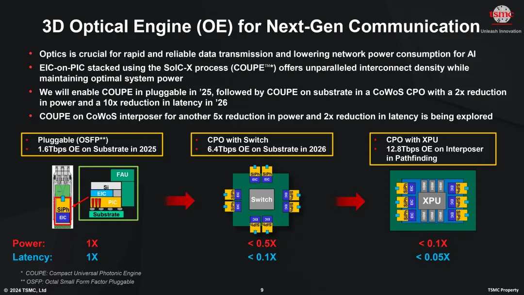
By adopting advanced 3D stacking technology, Taiwan Semiconductor is packaging electronic and photonic devices together. The first-generation product inserts into a standard optical fiber port at a speed of 1.6 Tbps, double that of current high-end Ethernet. The second-generation product integrates COUPE with processors into Taiwan Semiconductor's CoWoS package, increasing the speed to 6.4 Tbps. The ultimate outcome of the roadmap is the CoWoS 'COUPE Interposer' design, with fiber bandwidth reaching an astonishing 12.8 Tbps.
Regarding Taiwan Semiconductor's silicon photonics technology, although the company only recently announced its plans, according to **** media reports, they have actually been laying the groundwork for this for a long time.
**** media reported that by using the incoPat patent database to retrieve the current status of CPO co-packaged optical patent technology, it was found that Taiwan Semiconductor had long been laying out in this technological field and is currently one of the main patent holders in this field. For example, as early as 2013, Taiwan Semiconductor proposed the US9423578B2 patent, suggesting the use of optical signals instead of electrical signals for data transmission to address the increased latency caused by capacitance, inductance, or resistance in various types of ICs. Due to the early proposal of this technology, it has become a precedent for many other patents.
Earlier this month, Taiwan Semiconductor also participated in establishing a silicon photonics alliance, laying a solid foundation for the widespread adoption of this technology.
Taiwan Semiconductor's Vice President and General Manager, Xu Guojin, mentioned in his speech at the Alliance inauguration that the entire semiconductor industry has gone through 60 to 70 years of development, gradually focusing on CMOS (Complementary Metal-Oxide-Semiconductor) component technology application, which is also the processing technology utilized by silicon photonics for integrating photons and electrons. He pointed out that when CMOS became mainstream in commercial applications, industry development, from product design and research to upstream and downstream division of labor, became more clear, especially in terms of energy saving being a significant advantage.
Xu Guojin believes that currently optical components and silicon photonics components are still in the early stage of rapid development. With the massive computational and data transmission requirements of the AI era, energy consumption has become an important issue, and the introduction of silicon photonics components has become a key trend for data centers.
From the above report, we can also see that this former industry giant has truly become an unrivaled leader in the packaging field.
Editor/Rocky