
 该公司在声明中承认, Blackwell架构GPU存在良率问题,需要重新设计B200处理器部分设计以提升良率,因而下一代Blackwell架构GPU量产时间将推迟至2024年第四季度:
The 'ultimate challenge' of chip manufacturing.
If we summarize the 'root cause' of Nvidia's decline in one sentence, it is - advanced chips, the more powerful the performance, the more difficult the manufacturing.
On Wednesday, Nvidia reported strong quarterly sales and profits, but also pointed out that the manufacturing challenges of new chips led to a decline in profit margins. The company set aside a reserve of $0.908 billion in the last quarter. As a result, its stock price fell 6.4% on Thursday.
 The company acknowledged in a statement that the Blackwell architecture GPU has yield issues and needs to redesign part of the B200 processor to improve yield. Therefore, the mass production of the next generation Blackwell architecture GPU will be delayed until the fourth quarter of 2024.
We have adjusted the design of the Blackwell GPU to improve production yield. The production plan for Blackwell will start in the fourth quarter and continue until the 2026 fiscal year. We expect Blackwell products to generate billions of dollars in revenue in the fourth quarter.
We expect Blackwell products to achieve billions of dollars in revenue in the fourth quarter.
Nvidia did not provide detailed explanations of the specific reasons for the issue. However, analysts and industry executives believe that the engineering challenges mainly stem from the complex manufacturing process issues caused by the design of the Blackwell chip.
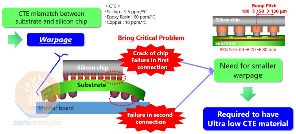
Analysis indicates that the giant size and complex design of Blackwell have brought unprecedented manufacturing complexity, and any defect in any component may lead to chip scrap, thereby affecting yield and profitability. In addition, the difference in thermal expansion coefficients of different parts of the chip may cause package warpage, affecting performance and reliability.
In order to improve yield, Nvidia has made adjustments to the Blackwell design and plans to increase production as scheduled. However, analysts believe that the complexity of the use of Taiwan Semiconductor's new chip interconnect technology and the inherent challenges of chip size will still be the main obstacles to mass production of Blackwell.
G. Dan Hutcheson, Vice President of industry analysis firm TechInsights, said,
"The problem lies in how to make the chips work together and improve yield. When the yield of each part of the chip is not high enough, everything can quickly deteriorate."
1. Complexity of the Blackwell chip
In order to maintain its leading position in the field of AI chips, Nvidia (NVDA) relies on the concept of "bigger is better." However, larger size brings greater manufacturing difficulties along with stronger performance.
Nvidia's latest AI chip, Blackwell, described by Jensen Huang as a "very, very big GPU," is indeed the largest GPU in terms of physical area. It consists of two Blackwell bare dies spliced together, adopts Taiwan Semiconductor's 4nm process, and has 208 billion transistors, which is 2.6 times that of the previous generation product.
UBS Group analysts stated in a report earlier this month that the main problem NVIDIA encountered on Blackwell was the over-complicated use of Taiwan Semiconductor's CoWoS-L new packaging method.
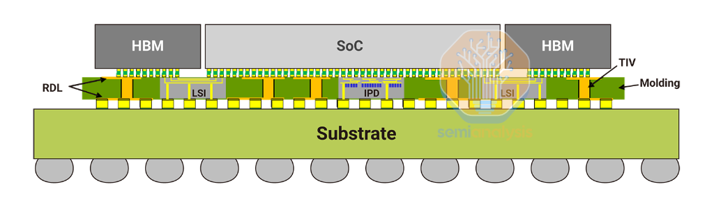
The semiconductor industry professional media semianalysis reported that this packaging technology uses RDL intermediate layers with local silicon interconnect (LSI) bridges to connect chiplets, with a transmission rate of about 10 TB/s. The placement accuracy requirements for these bridges are extremely high - any defect in a component can result in the scrap of a chip worth 0.04 million US dollars, thereby affecting the yield and profit.
In addition, the mismatch of the coefficients of thermal expansion (CTE) between the GPU chiplets, LSI bridges, RDL intermediate layers, and the main board substrates has led to chip warpage and system failures. It is reported that in order to improve the yield rate, NVIDIA had to redesign the top metal layer and bump of the GPU chiplets.
Huang Renxun emphasized in a conference call with analysts that no "functional changes" were needed for the Blackwell chips, and all adjustments were made to improve the yield rate.
Chief Financial Officer Colette Kress stated that NVIDIA is increasing the production of Blackwell as planned and expects Blackwell to generate billions of dollars in revenue for the company in the fourth quarter.
2. "Giant Chip" strategy
Such issues are not unique to nvidia. Industry insiders say that as chip manufacturers seek to increase processing power by enlarging chip sizes, these issues will become more and more common. Chip design changes made to eliminate defects or improve the yield rate are also very common in the industry.
AMD's CEO, Su Zifeng, also pointed out that as chip sizes continue to increase, manufacturing complexity will inevitably rise. The next generation of chips needs to make breakthroughs in energy efficiency and power consumption to meet the huge demand for computing power in ai datacenters.
"To make these technologies effective, a large amount of technical investment is needed," she said. "Will they become more complex and larger? Undoubtedly. This is our reality."
Of course, in order to break through the size limits of individual chips, nvidia combines two largest size chips to create Blackwell. This aggressive strategy has also attracted skepticism from competitors.
Competitor Cerebras Systems founder, Andrew Feldman, believes that the difficulty of developing multi-chip combination technology will grow exponentially. Cerebras Systems chose to develop giant single chips and launched ai cloud computing services based on this, attempting to challenge nvidia's market position.
"To do meaningful work in the ai field, a large amount of computing power is required, which means a large number of transistors, more than what a single chip can accommodate..."
The development of dual-chip technology is already difficult, the development of four-chip technology is even more challenging, while developing eight-chip technology is extremely difficult.
Whether Nvidia's giant chip strategy can ultimately succeed or not is still to be tested by the market. But what is certain is that the extreme challenges of chip manufacturing have just begun.
Editor/ping
