
As of now, new wafer fabrication projects in the United States are often delayed and the progress of many projects is uncertain. The problem of talent shortages is even greater.
Indeed, in recent years, the "Chip Act" in the United States has injected a stimulant into the revitalization of the domestic semiconductor industry, attracting many international giants to invest in building plants. However, behind this flourishing, the US semiconductor manufacturing industry has also gradually exposed many problems.
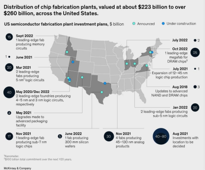
According to a report by the Center for Security and Emerging Technology (CSET), the construction speed of chip factories in the United States is one of the slowest regions in the world. CSET investigated the construction of wafer factories from 1990 to 2020 and found that the average time from the start of construction to production in the United States was 736 days, far higher than the global average (682 days), second only to Southeast Asia (781 days). By comparison, Taiwan is 654 days, South Korea is 620 days, and Japan is only 584 days.
As of now, the new semiconductor wafer fabs in the USA have seen frequent project delays, and the progress of many projects remains uncertain. It is also difficult to predict whether there will be abandoned projects in the future. The issue of talent shortage has also been exposed to a greater extent.
Postponed! Postponed! And postponed again!
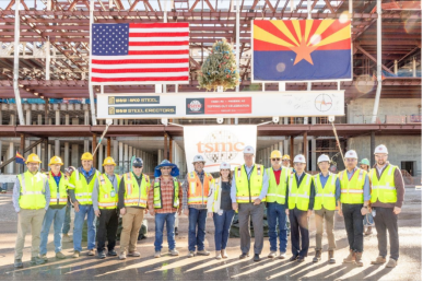
Taiwan Semiconductor's Arizona fab has been delayed.
Since announcing plans to build a factory in the United States in May 2020, TSMC has planned to build three factories in Arizona, but after four years, TSMC's first wafer factory has yet to produce any chips.
A review of TSMC's US plant construction plans:
On May 15, 2020, TSMC announced plans to build and operate an advanced semiconductor plant in Arizona, USA, with the mutual understanding and support of the federal government and the state of Arizona. TSMC is expected to spend approximately $12 billion on the project (including capital expenditures) between 2021 and 2029. At the time, the announcement was that the factory was planned to begin construction in 2021 and production was expected to begin in 2024. However, on April 8, 2024, the latest news from TSMC stated that TSMC's first wafer factory in Arizona is expected to start using 4nm technology for production in the first half of 2025, delaying it by a year.
On December 6, 2020, TSMC announced the construction of its second wafer fab in Arizona, which was initially expected to produce 3nm chips in 2026. However, the fab has also been delayed. TSMC said the second wafer fab will use the next generation of nanosheet transistors to produce the world's most advanced 2nm process technology and will begin production in 2028.
On April 8, 2024, TSMC announced that it plans to build a third wafer factory in Arizona with up to $6.6 billion in direct funding from the Chip and Science Act. With the completion of the third wafer factory, TSMC's cumulative investment in the United States will reach $65 billion, making it the largest foreign direct investment in US history. The third wafer fab will use 2nm or more advanced processes to produce chips and will begin production at the end of 2030.
At the time of building the factory, how enthusiastic, and now how much headache the cultural conflict is. According to the New York Times, including 12 TSMC employees, management and American workers at the company say that cultural clashes between **** executives and American workers have left both sides frustrated. TSMC is known for its strict working conditions, and it is not uncommon for people to be called to work in the middle of the night due to emergencies. But in Phoenix, some American employees quit after a dispute over expectations. In addition, American employees also complained about unnecessary meetings, and TSMC reduced the frequency and number of participants in an attempt to ease the tense situation. Currently, about half of the 2,200 TSMC employees in Phoenix are imported from Taiwan.
Intel Ohio fab delayed by two years
Intel is building fabs in multiple locations in the United States, including new wafer fabs and expansion factories in Arizona, New Mexico, Ohio, and Oregon, with investments of more than $100 billion expected over the next five years. In Arizona, Intel is building two cutting-edge semiconductor factories, each expected to cost between $15 billion and $20 billion; in New Mexico, Intel will invest $3.5 billion in its factory to produce its advanced semiconductor packaging technology, including Intel's breakthrough 3D packaging technology Foveros; in Ohio, Intel will invest more than $20 billion to build two new cutting-edge factories, the largest private sector investment in the state's history; and in Oregon, Intel plans to spend billions of dollars on expansion and modernization.
Due to market challenges and slow government funding, a report submitted by Intel to Ohio state officials on March 1st of this year showed that the production of the two wafer fabs in Ohio will be at least two years later than the original plan. The report shows that both semiconductor chip factories located in Columbus are expected to be completed by 2026 or 2027, and will not be put into operation until 2027 or 2028.
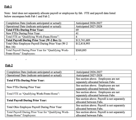
At the groundbreaking ceremony in September 2022, Intel stated that the two factories will begin operations in 2025. The total investment of the Intel Ohio project is 20 billion US dollars, but the report shows that Intel has invested 1.5 billion US dollars, plus a contract commitment of 3 billion US dollars, for a total investment of 4.5 billion US dollars, which accounts for one quarter of the total investment.

Samsung Taylor factory delayed for two years.
In 2021, Samsung announced a semiconductor cluster in Taylor, Texas, including two advanced logic wafer fabs and an advanced packaging facility, with a minimum investment of 17 billion US dollars. This is also Samsung's largest investment in the United States. Since operating in the United States in 1978, Samsung's total investment in the United States has exceeded 47 billion US dollars. It was expected that the Taylor plant would start mass production of 4nm in the second half of 2024.
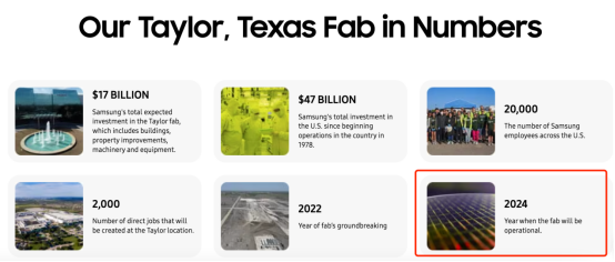
But on April 30 of this year, at Samsung's quarterly earnings conference, Samsung stated that the start of production at the Taylor plant has been postponed from the second half of 2024 to "possibly 2026".
On April 15, 2024, the U.S. Department of Commerce and Samsung Electronics signed a non-binding preliminary memorandum of understanding (PMT) to provide Samsung with a chip subsidy of 6.4 billion U.S. dollars. This will drive Samsung to reinvest 40 billion US dollars in the region.
Samsung further explained that the Taylor ecosystem will include two cutting-edge logic foundries focusing on mass production of 4nm and 2nm process technologies, a research and development factory dedicated to developing and researching leading production node technologies, and an advanced packaging factory for 3D high-bandwidth memory and 2.5D packaging.
Upstream suppliers' factories are also on hold.
Material manufacturers and equipment manufacturers jumped into the construction of production plants after TSMC and Intel announced their plans to build factories in the United States, as a lot of chemicals and materials are required to build a wafer fab. LCY Chemical, Solvay, Chang Chun Group, KPPC Advanced Chemicals (Kanto-PPC), and Topco Scientific, chemical and material manufacturers in the supply chain, followed suits to build production plants. They also bought land in the southeast of Phoenix's Casa Grande town, not far from Intel and TSMC wafer fab.
Nikkei Asia reported earlier this year that the construction of these essential facilities for building a complete chip supply chain has been put on hold or significantly scaled back, indicating the challenge of rebuilding the US chip supply chain is greater than expected.
Most affected companies blame project delays on soaring building materials and labor costs, as well as a shortage of construction workers.
Some material suppliers indicate that the cost of building a factory in Arizona is four to five times higher than building one in Asia, and the profit margin of chemical suppliers is lower than that of chip manufacturers, making them more sensitive to the rising costs. Furthermore, seeing that Intel's and TSMC's expansion progress is slower than expected, local demand does not require so much local supply. For the chemical industry, there must be economies of scale to achieve economic benefits.
Compared with complex wafer fabs, material production plant construction is faster, which means they can build factories when customers are ready. Although material factories are also included in the US semiconductor subsidy law, according to the procedure of the US Department of Commerce, financial support will only be provided to material and chemical suppliers after the subsidy decisions of these chip manufacturers have been made. Therefore, they choose to suspend the construction plan and transport chemicals to the United States through logistics to meet local demand.
Applied Materials is a global semiconductor equipment leader and the largest semiconductor equipment supplier in the United States. In August, according to Bloomberg, applied materials, a global semiconductor equipment leader, expected chip subsidies for its long-awaited R&D center application to be rejected. This also shows that material and equipment companies have difficulty obtaining subsidies.
Who got the most chip subsidies?
Among the current beneficiaries of chip subsidies, Intel is undoubtedly the largest beneficiary.
The Chip Act, promulgated in August 2022, plans to allocate more than $52.7 billion to support research and development, manufacturing, and workforce development of semiconductors in the United States. Of this, $39 billion will be used to directly subsidize semiconductor manufacturers.
On March 20th, the US Department of Commerce signed a non-binding memorandum of preliminary terms with Intel, planning to provide $8.5 billion in direct funding subsidies and $11 billion in federal loan guarantees through the Chip and Science Act to promote semiconductor projects in Arizona, New Mexico, Ohio, and Oregon.
On February 19, 2023, the US government announced that it will provide Global Foundries with $1.5 billion in funding to build a new semiconductor factory in Malta, New York, and expand production scale in local production facilities in Burlington, Vermont. In addition, $1.6 billion in loans will also be provided.
On April 8, 2024, the US Department of Commerce announced that it will provide TSMC with a $6.6 billion direct funding subsidy and a $5 billion low-interest government loan to support TSMC's construction of three new chip factories in Arizona.
On April 15th, the US Department of Commerce also announced a $6.4 billion direct subsidy for Samsung to support the construction of a computer chip manufacturing and R&D industry cluster in Texas.
On April 25th, Micron Technology announced that it will receive $6.14 billion in direct funding to build two DRAM wafer factories in New York and a new DRAM wafer factory in Idaho.
On July 26, outsourcing semiconductor packaging and testing supplier Amkor Technology announced that it has received $0.4 billion in direct funding support and a $200 million loan. Amkor Technology announced in November 2023, the first US domestic OSAT facility construction plan in Peoria, Arizona. Amkor Technology expects to invest approximately US$2 billion and employ approximately 2,000 employees in the new facility. Once completed, it will be the largest outsourced advanced packaging and testing facility in the United States. It is worth mentioning that the United States plans to allocate a total of US$1.6 billion in the packaging field.
In addition, Microchip Technology in the United States received a government grant of $0.162 billion to double the output of mature node semiconductor chips and MCUs in two domestic factories.
Chip subsidies cannot shake the slow pace of construction in the United States. The construction of wafer fabs requires long-term guarantees of resources such as land, water, electricity, and personnel. Moreover, these subsidies do not know when they will be in place.
The biggest challenge facing the construction of wafer fabs in the United States
The biggest challenge in building wafer fabs in the United States is the shortage of workers. This includes two types of talents: construction talents and technical personnel needed to operate wafer fabs.
According to a report by McKinsey, the United States has never built wafer fabs on a large scale for more than 20 years, and few domestic construction contractors have the experience, capabilities, and professional knowledge required to complete these specialized projects. In addition, semiconductor companies must also compete with companies in multiple industries (including residences) to compete for various construction workers (from earthmoving experts to skilled electricians), and the US labor market is already very tight.
Once the wafer fabs are built, they will face a shortage of employees. Whether it is local manufacturers or foreign wafer fabs, their construction sites are relatively concentrated. For example, TSMC and Intel are both building factories in Arizona. The reason why Arizona and Texas attract investment is because they already have wafer fab ecosystems, and local governments have always provided incentives and helped coordinate this process. In addition to huge incentives, Ohio is becoming an ideal location, such as Samsung's investment of more than $20 billion in the Columbus fab, and New York State also offers incentives to encourage wafer fab construction. Other investment-attracted states include Indiana, New Mexico, Oregon, Utah, and Virginia. The concentration of wafer fabs also makes talent competition even fiercer.
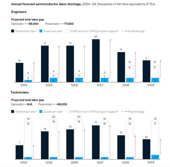
According to a new study by McKinsey, as far as the current investment announced by the United States is concerned, it far exceeds the available talent supply. By 2032, to quickly expand the US semiconductor industry, the total public and private investment will exceed $250 billion. This investment will bring new job vacancies for more than 160,000 engineering and technical support positions, as well as additional vacancies for related construction processes.
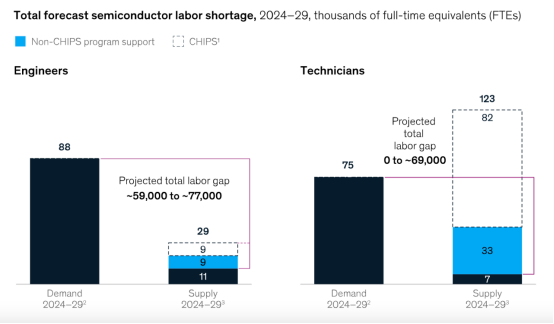
McKinsey also pointed out that although there are approximately 1,500 engineers joining the semiconductor industry every year under the promotion of the Chip Act, they only account for 3% of the engineering graduates entering engineering positions. In contrast, by 2029, demand for semiconductor engineers is expected to reach 88,000, and the potential talent gap is evident.
Without sufficient technical personnel and engineers, factories cannot operate at full capacity. In turn, the productivity of manufacturers will also decline, which may increase the selling price of chips.
In response, the United States has also launched some programs to cultivate young talents, such as:
Purdue University led the academic project SCALE funded by the Department of Defense to train students from 22 universities to become microelectronics engineers, hardware designers, and manufacturing experts.
Samsung Austin Semiconductor Corporation is collaborating with Taylor Independent School District to develop valuable skills for future career development and provide internship opportunities for students.
Micron Technology is collaborating with 11 universities (6 in the United States and 5 in Japan), spending $60 million to provide 5,000 students with cleanroom experiential learning and memory-related research opportunities each year.
Michigan Economic Development Corporation (MEDC) invested $3.6 million to promote semiconductor training and education, distributed to four higher education institutions in the Detroit metropolitan area: Oakland University, University of Michigan, Washtenaw Community College, and Wayne State University. Furthermore, MEDC provided $838,000 to Michigan Technological University on the Upper Peninsula of Michigan to expand its semiconductor training and education through microcertificate courses.
In addition, there are some short-term technical staff training programs, such as:
Mesa Community College in Maricopa County, Arizona plans to train 4,000 to 6,000 technical personnel through cooperation with Intel and Taiwan Semiconductor Manufacturing Company. Both companies have made large investments in semiconductor manufacturing plants.
Oregon and Washington counties also support Portland Community College, which is partnering with Intel to provide paid ten-day training courses for semiconductor technicians.
Michigan provided $1.5 million to the SEMI Foundation to support job seekers and attract semiconductor talent through a registered apprenticeship program.
GlobalFoundries is partnering with Hudson Valley Community College and the State University of New York to provide a full-time paid apprenticeship program of approximately 18 months at its manufacturing base in Malta, New York, where apprentices will receive on-the-job training and participate in courses funded by the State University of New York.
Although these crash courses can temporarily alleviate the situation, chip factories still need a large number of high-tech talents. These highly skilled talents are even more critical.
In fact, according to McKinsey's estimation, considering the current growth rate and predicted demand, by 2029, the potential talent gap in the engineering and technical workforce in the semiconductor industry may reach approximately 59,000 to 146,000 workers. The lower end of the forecast range represents the Office of CHIPS Project's estimate of complete realization of its supported projects, while the higher number reflects the potential situation when projects or funding levels do not meet expectations.
In conclusion,
With such a big move, what will be the level of semiconductor manufacturing in the United States? According to SIA, it is expected that by 2032, the United States' share of global semiconductor production will increase from the current 10% to 14%, which is still far from the 37% 30 years ago. The United States' goal of semiconductor manufacturing still has a long way to go.
Editor/ping