
Hitachi Ltd., Kyushu University, RIKEN - National Research and Development Agency, and HREM Co., Ltd. have developed a method using Hitachi's atomic resolution holography electron microscope to observe the magnetic field of heterogeneous samples such as magnetic multilayers where their structure and composition have been difficult to observe so far due to its inhomogeneity, and succeeded in observing the lattice-plane-resolved magnetic field for the first time in the world through this method. The research partners have cooperated with National Institute of Advanced Industrial Science and Technology (AIST) and National Institute for Materials Science (NIMS) as well.
This achievement was made possible by improving the precision of electron holography and developing technology to automatically correct the focus after imaging. This makes it possible for the first time to observe the magnetic field at the atomic layer level at the boundary (interface) between localized materials, which greatly affects the properties of materials containing heterogeneous samples and the characteristics of electronic devices. It will contribute to the development of basic science through elucidation of magnetic phenomena occurring at the atomic layer level, as well as making a contribution to the realization of a carbon-neutral society by developing high-performance magnets and functional materials for electrification and developing energy-saving devices required in our daily life to reduce overall energy consumption.
This research achievement was published online in the international academic journal "Nature" on July 4, 2024 (Thu.) at 0:00 (Japan Time).
Background of the study
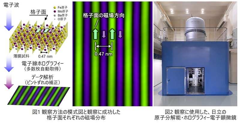
Electronic devices and motors are used in various applications such as smartphones, computers, automobiles, railways, power plants, and support our daily lives. Since many of their functions and performances are related to the arrangement of atoms, the smallest unit of matter, and the behavior of electrons, a technology for observing materials with ultra-high atomic resolution is required for the emergence of new functions and further improvement of their performance. So far, Hitachi has been developing holography electron microscopes since 1966 to directly observe tiny electric fields and magnetic fields in order to meet this requirement, and developed Hitachi's atomic resolution holography electron microscope with the support of the "Funding Program for World-Leading Innovative R&D on Science and Technology (FIRST)" in 2014 (Figure 2). In 2017, they achieved a resolution of 1 nm*5 or less, enabling magnetic field observation at the atomic layer level, in collaboration with RIKEN*. However, further high-resolution imaging required precision improvement of the microscope and correction of small image blur caused by imaging.
Therefore, this joint research team has developed a technology that solves these problems and allows the observation of the magnetic field for each lattice plane for heterogeneous samples such as magnetic multilayers that have been difficult to observe so far.
Features of the development technology.
- Technology to acquire a large number of images automatically to improve the precision of electron holography.
The accuracy of electron beam holography improves by increasing the number of image data acquired. Based on the technology of separating electric field information and magnetic field information with high accuracy through observation results of electron beam holography developed in 2017, we have developed a technology that automatically acquires more than 10,000 images in about 8.5 hours while achieving ultra-high resolution by automating control and adjustment of the microscope during data acquisition and speeding up shooting. The operating income of products worth 10-30 billion yuan is 401/1288/60 million yuan, respectively. - Digital aberration correction technology that automatically corrects slight focus discrepancies to obtain high resolution.
In order to obtain high resolution, it is necessary to correct the small focus discrepancies remaining in the imaging data. The idea of correcting focus after imaging is theoretically established when Dennis Gabor invented electron beam holography in 1948, but there has been no technology to correct it automatically until now. This time, we applied a method*7 that corrects focus by analyzing electron waves obtained by changing focus to electron beam holography, and succeeded in automatic correction by developing a unique algorithm that reduces the influence of noise in experimental data.
This technology was applied to atomic-resolution holography electron microscopy to observe a magnetite (Ba2FeMoO6 crystal) with magnetic fields of different sizes and directions for each atomic layer, and it was possible to observe the magnetic fields of each lattice plane inside the substance with a resolution of 0.47 nm, the highest performance in the world*8, allowing observation of non-uniform samples.
With this achievement, it is expected that high-function materials and energy-saving device development will be accelerated, making it possible to observe the relationship between interface structure and magnetic field in the device and material in detail, and contributing to the development of basic to advanced devices by jointly utilizing this equipment through the support of the Ministry of Education, Culture, Sports, Science and Technology (MEXT), Advanced Research and Development Support Program, and National Institute for Materials Science.
Comment by Yohki Tokura, Director of the Strong Correlation Physics Research Group, Center for Emergent Matter Science, RIKEN
This achievement is a new electron microscope method that can directly observe magnetic fields at the lattice plane level, and is expected to contribute to the development of materials science. I am convinced that the method will open up new avenues for the construction of innovative electronics with greatly reduced power loss and the development of devices by utilizing this method in the future.
Some of this research was supported by Grants-in-Aid for Scientific Research (JPMJCR1664) from the Japan Society for the Promotion of Science (JSPS) through the Independent Researcher and the Strategic Basic Research Programs of the Japan Science and Technology Agency (JST), "Development of Intelligent Measurement and Analysis Techniques by the Fusion of Measurement Technology and Advanced Information Processing."
Introduction of Hitachi's atomic-resolution holography electron microscope.
- Overview explanation.
- Introduction video.
- February 18th, 2015 Hitachi news release "Hitachi develops an atomic-resolution holography electron microscope, achieving the highest resolution of 43 picometers in the world".
Hitachi is promoting a Social Innovation Business to achieve a sustainable society with data and technology. Under a three-sector business structure of Digital Systems & Services to support customers' DX, Green Energy & Mobility to contribute to the realization of a decarbonized society through energy and railway businesses, and Connective Industries to provide solutions that connect products in a wide range of industries digitally, we solve our customers' and society's issues through Lumada solutions that utilize IT, OT, and products, driven by digital, green, and innovation. We aim to grow through co-creation with customers. The sales revenue of the three sectors in 2023 is 8.5643 trillion yen, and as of March 2024, we have 573 consolidated subsidiaries and around 270,000 employees worldwide.
About Hitachi
Hitachi is promoting a Social Innovation Business to achieve a sustainable society with data and technology. Under a three-sector business structure of Digital Systems & Services to support customers' DX, Green Energy & Mobility to contribute to the realization of a decarbonized society through energy and railway businesses, and Connective Industries to provide solutions that connect products in a wide range of industries digitally, we solve our customers' and society's issues through Lumada solutions that utilize IT, OT, and products, driven by digital, green, and innovation. We aim to grow through co-creation with customers. The sales revenue of the three sectors in 2023 is 8.5643 trillion yen, and as of March 2024, we have 573 consolidated subsidiaries and around 270,000 employees worldwide.
- Hitachi's website
- About Lumada
Contact
Hitachi Research & Development Group
- Inquiries about R&D
Kyushu University National University Corporation
Public Relations Division
Phone: 092-802-2130
- E-mail: koho@jimu.kyushu-u.ac.jp
RIKEN Center for Emergent Matter Science Strong Correlation Physics Research Group, Yohki Tokura Group Director.
Public Relations Department Press Officer
Telephone: 050-3495-0247
- E-mail: ex-press@ml.riken.jp
Limited Liability Company HREM (HREM Research Inc.)
- E-mail: support@hremresearch.com
The information in this news release (product prices, product specifications, service contents, release dates, contact information, URLs, etc.) is current as of the announcement date. Please note that it may be changed without notice and there is a possibility that the information may differ from the search date, so please be forewarned. For the latest contact information, please refer to the list of inquiries.