
It is expected that the compound annual growth rate (CAGR) of Taiwan Semiconductor's non-crystalline wafer revenue will reach 31% from 2023 to 2026; Rubin architecture may adopt 3D SoIC packaging technology.
$Taiwan Semiconductor (TSM.US)$Recently, there have been numerous developments, from raising prices for advanced processes to entering the "square substrate" market.
Recently, Morgan Stanley released a report on Taiwan Semiconductor, summarizing in detail the latest developments in CoWos, PLP technology and 3D SoIC.
- CoWos packaging: Taiwan Semiconductor expects that by the end of 2026, the monthly CoWoS wafer production capacity will be approximately 60,000 pieces; compared with the previously disclosed CoWoS packaging production capacity of 26-28 thousand pieces/month at the end of 2024, it will more than double.
- Panel Level Packaging (PLP): This technology is related to the recently market attention to "square substrate". Currently in the research and development stage, large-scale production will take several years.
- 3D SoIC packaging: it is expected to increase production capacity from the second half of 2025, and Rubin architecture may adopt 3D SoIC packaging technology.
I. CoWoS production capacity update
In a recent technical symposium, Taiwan Semiconductor stated: From 2022 to 2026, the CoWoS technology production capacity is expected to grow rapidly at a compound annual growth rate of more than 60%. By the end of 2026, the monthly CoWoS wafer production capacity will be approximately 60,000 pieces.
At present, Taiwan Semiconductor's monthly CoWoS production capacity is about 15,000 pieces, and it is expected to increase to 26-28 thousand pieces/month by the end of 2024.
At the same time, in 2024, Taiwan Semiconductor plans to invest 28-32 billion US dollars, of which about 10% will be used for advanced packaging technology.
Morgan Stanley analysts pointed out that strong packaging demand will become the main driving force for the rapid growth of Taiwan Semiconductor's non-crystalline wafer revenue in the next few years:
- It is expected that the compound annual growth rate (CAGR) of Taiwan Semiconductor's non-crystalline wafer revenue will reach 31% from 2023 to 2026;
- By 2023, non-crystalline wafers are expected to account for 13% of Taiwan Semiconductor's total revenue;
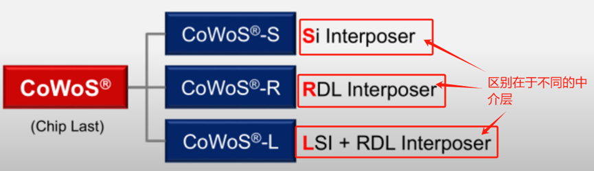
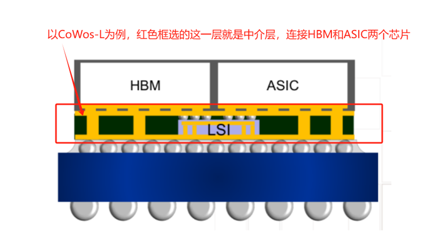
1) CoWoS-L packaging
Morgan Stanley pointed out that Taiwan Semiconductor is accelerating the expansion of its CoWoS technology, focusing on adapting to the increasingly large size of AI chip demand, especially CoWoS-L technology.
CoWoS packaging technology is now divided into three types: CoWoS-S, CoWoS-R and CoWoS-L. Their main difference is the design of the intermediate layer, which is a key layer for connecting chips.
As the size of AI chips increases, the previous CoWoS-S technology using silicon intermediate layers has encountered yield problems.
To deal with this challenge, Taiwan Semiconductor has introduced CoWoS-L technology, which uses LSI+RDL intermediate layers to effectively solve the yield problem of large-size chips.
Morgan Stanley expects that in the future, Taiwan Semiconductor's development of CoWoS technology will mainly focus on CoWoS-L to cope with the increasing area demand of AI chips.
II. Panel Level Packaging (PLP) technology
According to Morgan Stanley, Taiwan Semiconductor is researching panel-level packaging (PLP) technology, but large-scale production will still take a few years.
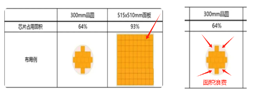
PLP packaging is a packaging scheme that rearranges chips on a larger rectangular panel (see left side of the figure below).
Currently, Taiwan Semiconductor uses circular wafer substrates, which results in wasted space (see right side of the figure below).
According to Nikkei Asia, Taiwan Semiconductor is exploring rectangular substrates of 510㎜ × 515㎜ due to the increased computing demand brought by AI.
The effective area of rectangular substrates is more than three times larger than that of circular wafers, which is expected to significantly improve Taiwan Semiconductor's production capacity.
However, compared with circular substrates, there are issues with uneven photoresist coating and fragility of square substrates.
Morgan Stanley pointed out that it will still take several years to achieve large-scale production of PLP packaging technology through technical breakthroughs.
III. 3D SoIC advanced packaging
3D SoIC is an advanced packaging technology developed by Taiwan Semiconductor, focusing on achieving high-density chip vertical stacking (as opposed to CoWoS technology, which is mainly horizontal stacking).
Morgan Stanley pointed out that currently, 3D SoIC technology is still relatively niche in the market, only adopted by AMD in its Ryzen 3D and MI300 AI accelerators.
It is expected that starting from the second half of 2025, Taiwan Semiconductor will gradually increase the production capacity of 3D SoIC. By the end of 2025, the expected monthly production capacity of 3D SoIC will reach about 12,000 to 14,000 wafers; by the end of 2026, it is expected to increase to 20,000 wafers per month.
In addition, Morgan Stanley speculates that Nvidia's Rubin architecture and Apple's M5 processor may adopt 3D SoIC technology.
Editor/Somer