
Source: Tencent Technology Author: Morris.Zhang, PMO director of back-end products at a factory
Some time ago, the well-known hardware website Tomshardware quoted people familiar with the matter as saying,$NVIDIA (NVDA.US)$In order to ensure the supply of GH200 and H200 this year, a budget of 1.3 billion US dollars was set, and part of the HBM3e memory production capacity was reserved from Micron and SK Hynix.
However, since there is no reasonable calculation of this set of data, the credibility of the 1.3 billion budget has yet to be confirmed, but what is certain is that this budget cannot short the production capacity of global HBM in 2024.
Its value is that it can help Nvidia seize the “monopoly computing power” window in the first half of 2024 — the first product is marketed, then it can seize market share first.
1. 2024, about 56 million HBM units shipped
In 2024, the total production capacity of SK Hynix, Micron, and Samsung will expand to 750,000 wafers. According to current industry data, the yield of HBM3e is about 90%, and each wafer can be cut. The total global HBM production capacity in 2024 is roughly 56 million pieces (12 layers + 8 layers), but large-scale production capacity is concentrated in the second half of the year, and the proportion is slightly smaller in the first half of the year.
Based on the 2024 CoOS package production capacity estimate:
In terms of GPU-HBM vertical packaging production capacity, as of the fourth quarter of 2024, the total packaging production capacity of global CoWOS is estimated to be about 300,000 wafers, including$Taiwan Semiconductor (TSM.US)$There are about 270,000 pieces, and Amkor is about 40,000 pieces. Since the process nodes of these wafers are concentrated at 5nm and 3nm, the current yield is about 38%. Conservatively, a single wafer can cut 30 GPU chips, that is, for the whole of 2024, GPU products packaged via Cowos worldwide have a production capacity of about 9 million pieces. According to the standard calculation of a single GPU logic chip with 6 HBM memory particles (AMD MI300 with 8 HBMs), the global demand for HBM memory in 2024 is over 54 million GPUs (mainly 12 layers).
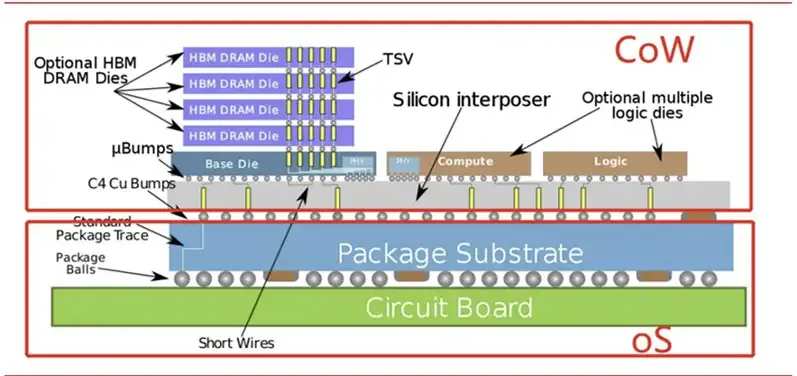
Note: CowOS, commonly known as 2.5d package, is Chip on Wafer on Substrate. It is used to meet the interconnection of multiple computing chips and the stacking implementation of memory chips under relatively ideal electrical rules.
Currently, the channel unit price for 12-layer HBM pellets is about $250+ each. If the 1.3 billion budget is true, Nvidia can only order 5.2 million pieces, accounting for only 1/10 of HBM's total annual production capacity.
In fact, according to estimates from packaging data, Nvidia has scheduled a CoOS production capacity of more than 140,000 wafers in 2024, of which TSMC is divided into 120,000 wafers as the “main supplier” and Amkor is divided into 20,000 to 30,000 wafers as a “secondary supplier”, with an overall production capacity of nearly 4.5 million units.
According to the 1:6 ratio of each GPU logic chip and storage particle, that is, Nvidia needs about 27 million HBMs throughout the year. Based on the cost estimate of a single unit of 250 US dollars, this means that Nvidia can predict the cost of purchasing HBM chips for the whole year to 6.8 billion US dollars, far exceeding the 1.3 billion US dollar budget previously disclosed by the media.
Note: Consumer graphics cards such as the Nvidia RTX series that use GDDR6 particles are naturally not included in CoWOS production capacity; the Nvidia production capacity mentioned above refers specifically to the Hopper series and the B200 of the Blackwell architecture. From this, it is estimated that Nvidia's HBM particle order demand in 2024 is 27 million units.
II. What is behind the tight production capacity of HBM
As of the fourth quarter of 2024, the planned production capacity of each GPU supercomputing product corresponding to HBM particle packaging is about 9 million units. Combined with the production expansion plans of the three Hynix/Samsung/Magiguang memory manufacturers in 2025, it is nearly 60 million HBM units (mainly 12 layers, 8 layers slightly less). These two supply data are consistent, and also indicate that the production capacity of CowOS and HBM for 2024-2025 is sufficient.
However, although there is no shortage of production capacity, after all, the above data is an “annual plan”. In fact, most production capacity will not be released until the fourth quarter. Of course, the production capacity scheduled by each company is the sooner the better. Timeliness is a key condition. The opportunity window at the beginning of the first half of the year is even more important. If production only starts in the second half of the year, then the product will have to wait until the next year to enter the channel.
Also, regarding the expansion of CoWoS production capacity, it currently mainly depends on the production capacity of TSMC and Amkor, such as Taiwan$United Microelectronics (UMC.US)$Although production lines such as GF and GF can also be used as intermediaries at the leading 65nm stage, due to a lack of advanced process coverage, that is, they are unable to OEM advanced process logic chips and intermediaries, nor can they achieve a one-stop full CoWOS stack. Currently, the most likely catcher is Samsung.
Samsung plans to introduce a full-stack CowOS package, commercialized and named I-CUBE/H-CUBE, to compete with TSMC for orders; however, Samsung is not yet able to offer production capacity in 2024, and 2025 may be more beneficial to Samsung. As an IDM manufacturer that supplies HBM and Cowos at the same time, its process characteristics and price advantages are obvious. (In the future, Samsung will also launch the X-CUBE 3D package, collectively known as SAINT, or Samsung's advanced packaging technology.)
Also, if Intel's foundry business successfully operates independently in 2025, its Intel Foveros packaging solution is also worth watching.
Currently, we see that HBM's global inventory and channel turnover is very tight. The actual reason is that the current HBM3e supplier is SK Hynix, which coincides with the peak demand for HBM brought about by the rapid development of large models, which in turn causes an imbalance between supply and demand, but this imbalance will slow down as production capacity expands.
However, there is one thing to be aware of. Storing pellets is a standard SKU, and there is no need for customized customization of the particles themselves, so this category has created a so-called spot market. Standard stock can be distributed normally through channels or distribution platforms. That is, if all of the planned production capacity of SK Hynix, Micron, and Samsung memory factories are successfully released in 2024, the inventory of agents in all regions of the world will be sufficient, and countless secondary channels/sub-agents can resell indefinitely.
Therefore, as long as the stock inventory is sufficient and the price trend improves, the spot market can always pick up goods and evolve into a DRAM spot channel business format. This is an industrial characteristic of memory particles.
This raised a very interesting topic. What if, due to special reasons, a company cannot order through the three companies mentioned above?
The spot market is a channel — specific companies can purchase HBM particles from the spot market and then adapt to controllers, I/O, and logic packages.
If HBM memory cannot be purchased in the spot market, 2D-DRAM particles can also be purchased from the spot market, and then an HBM device with low specifications can be stacked through a TSV vertical hole and TCB hot press bonding (hybrid bonding will be required for more layers in the future) packaging process.
Of course, the ultimate goal is to develop self-developed memory particles to achieve independent industrialization of HBM.

3. CoWoS threshold: industrial chain and yield
Referring to the current GPU chip configuration, if the CoWOS package structure is missing, the HBM will not even be placed anywhere.
Currently, there are several categories of CoWoS capacity suppliers to choose from around the world:
The first is TSMC CoWoS;
Second, TSMC completes the manufacture of the wafer and the front intermediate layer (that is, the “CoW” part of CoWOS, stacking+interconnect), and then hand it over to its own packaging factory (such as idle InFO production capacity) or a cooperative third party OSAT packaging factory, commonly known as an outsourced packaging factory, to complete the “on Substrate” part, that is, encapsulated on the substrate;
Third, production intermediaries can be commissioned from UMC and GF, and then sent to OSAT production lines such as Amkor or Sun Moon Light to complete the “WoS” part. However, as mentioned earlier, these two process nodes are basically around 65nm. They cannot OEM advanced advanced process logic chips and intermediaries, nor can they complete a one-stop CoWoS full stack;
The fourth is Samsung I-Cube/H-Cube and Intel Foveros. Both companies can complete full-stack CoOS delivery, but they have yet to develop production capacity;
Fifth, there are also some domestic CoWOS capabilities, but almost all of them are Cow+WoS process connections, that is, UMC, GF + Amkor, and Sun & Moonlight models.
Compared to other manufacturing processes, CoWoS does not have an extremely cutting-edge technical threshold; the only key is that it must guarantee high yield under a highly compact process.
Because at the packaging level, if the product has high defects/failures, then devices such as HBM stacked and connected on top will become irretrievably lost, and manufacturers that can balance high process nodes and yield. Currently, only TSMC can satisfy them.
As far as CoW+WoS production capacity alone is concerned, the world can offer a lot of production capacity (especially WoS manufacturers), but there is not much production capacity that can be applied to the process/yield of advanced computing chips.
The reason for the above yield threshold is the process:
Taking the WoS yield as an example, the main difficulty is that the size of the intermediate layer of the package should be strictly limited, that is, the area of the silicon interlayer must be larger than the sum of the sizes of the 2 or more bare crystals on it. However, as this size became larger and larger, the fifth generation of CoWOS even supported the expansion of the intermediate layer to 2,500 mm² through a “2-way lithography stitching approach”. The resulting process risks were on-wafer, that is, when stacked on silicon wafers, problems such as edge distortion and vertical convex angles, which led to poor sealing and testing. TSMC's CoWoS process has been working together for more than 10 years, and has accumulated a large number of knowhow to obtain today's reliable high yield.

For OSAT specialty packaging plants (including Amkor/Sun Moon Light, etc.), the slow increase in process yield is also related to the separate manufacturing of the interlayer in the previous stage. Although CoW+wOS is a reasonable division of labor in the industrial chain, increasing the yield of the two joint products requires the simultaneous development of the two processes.
Currently, the mainland's advanced logic chips and intermediaries are basically composed of$SMIC (00981.HK)$After manufacturing, it is outsourced to OSAT's professional packaging factory to complete WOS packaging testing; if SMIC's production capacity is not available, UMC and GF can also be outsourced.
In the future, most 2.5D packaging in the world will probably be a front-road+back-channel cooperation model; the front-end fabs provide an intermediary layer for CoW, and a carrier board for WoS in the future. In addition, CowOS will also be applied more to other scenarios. Most future products involving AI-HPC will rely on CoWOS packaging. Looking at 2.5D/3D packaging at present, fabs still have an advantage over OSAT.
IV. Conclusion
With the AI-HPC industry's high demand for HBM memory, the product audience, product value, and market space of this device have all soared. Today, the unit price of HBM is several times that of traditional DRAM, and about 5 times that of DDR5.
As mentioned earlier, the current channel unit price for 12-layer HBM granules is already 250 US dollars/piece, which is a slight increase compared to 2023.
Another measurement perspective: Currently, on AI-HPC calculation chips, the total cost of 6 16GB HBM3 particles is usually about 1,500 US dollars, which is equivalent to 15.6 US dollars/GB; converted to H100 SXM5 boards, 6 HBM3 80GB, equivalent to 18.75 US dollars/GB, accounting for about 50% + of the material cost of the entire chip.
One set of data comes from Yole: the overall composite growth rate of advanced packaging in the next 5 years will be 40%, of which 3D packaging will grow by more than 100%; and in five years, close to 40% of HBM will be based on hybrid bonding packaging.
Therefore, regardless of whether they are overseas or mainland manufacturers, the potential market space for the industrial directions “HBM, CoW, TSV/hybrid bonding” mentioned above is broad, and we expect domestic manufacturers to have mature yields and the possibility of entering overseas markets. At the same time, with the boom in the AI-HPC market, driven by this, it is expected that HBM's share in the pan-DRAM market will increase dramatically. HBM's share of total DRAM market capacity is expected to rise from 2% in 2023 to 5% in 2024, and more than 10% by 2025.
edit/lambor