
Source: Semiconductor Industry Watch. At yesterday's Conputex conference, Dr. Lisa Su released the latest roadmap. Afterwards, foreign media morethanmoore released the content of Lisa Su's post-conference interview, which we have translated and summarized as follows: Q: How does AI help you personally in your work? A: AI affects everyone's life. Personally, I am a loyal user of GPT and Co-Pilot. I am very interested in the AI used internally by AMD. We often talk about customer AI, but we also prioritize AI because it can make our company better. For example, making better and faster chips, we hope to integrate AI into the development process, as well as marketing, sales, human resources and all other fields. AI will be ubiquitous. Q: NVIDIA has explicitly stated to investors that it plans to shorten the development cycle to once a year, and now AMD also plans to do so. How and why do you do this? A: This is what we see in the market. AI is our company's top priority. We fully utilize the development capabilities of the entire company and increase investment. There are new changes every year, as the market needs updated products and more features. The product portfolio can solve various workloads. Not all customers will use all products, but there will be a new trend every year, and it will be the most competitive. This involves investment, ensuring that hardware/software systems are part of it, and we are committed to making it (AI) our biggest strategic opportunity. Q: The number of TOPs in PC World - Strix Point (Ryzen AI 300) has increased significantly. TOPs cost money. How do you compare TOPs to CPU/GPU? A: Nothing is free! Especially in designs where power and cost are limited. What we see is that AI will be ubiquitous. Currently, CoPilot+ PC and Strix have more than 50 TOPs and will start at the top of the stack. But it (AI) will run through our entire product stack. At the high-end, we will expand TOPs because we believe that the more local TOPs, the stronger the AIPC function, and putting it on the chip will increase its value and help unload part of the computing from the cloud. Q: Last week, you said that AMD will produce 3nm chips using GAA. Samsung foundry is the only one that produces 3nm GAA. Will AMD choose Samsung foundry for this? A: Refer to last week's keynote address at imec. What we talked about is that AMD will always use the most advanced technology. We will use 3nm. We will use 2nm. We did not mention the supplier of 3nm or GAA. Our cooperation with TSMC is currently very strong-we talked about the 3nm products we are currently developing. Q: Regarding sustainability issues. AI means more power consumption. As a chip supplier, is it possible to optimize the power consumption of devices that use AI? A: For everything we do, especially for AI, energy efficiency is as important as performance. We are studying how to improve energy efficiency in every generation of products in the future-we have said that we will improve energy efficiency by 30 times between 2020 and 2025, and we are expected to exceed this goal. Our current goal is to increase energy efficiency by 100 times in the next 4-5 years. So yes, we can focus on energy efficiency, and we must focus on energy efficiency because it will become a limiting factor for future computing. Q: We had CPUs before, then GPUs, now we have NPUs. First, how do you see the scalability of NPUs? Second, what is the next big chip? Neuromorphic chip? A: You need the right engine for each workload. CPUs are very suitable for traditional workloads. GPUs are very suitable for gaming and graphics tasks. NPUs help achieve AI-specific acceleration. As we move forward and research specific new acceleration technologies, we will see some of these technologies evolve-but ultimately it is driven by applications. Q: You initially broke Intel's status quo by increasing the number of cores. But the number of cores of your generations of products (in the consumer aspect) has reached its peak. Is this enough for consumers and the gaming market? Or should we expect an increase in the number of cores in the future? A: I think our strategy is to continuously improve performance. Especially for games, game software developers do not always use all cores. We have no reason not to adopt more than 16 cores. The key is that our development speed allows software developers to and can actually utilize these cores. Q: Regarding desktops, do you think more efficient NPU accelerators are needed? A: We see that NPUs have an impact on desktops. We have been evaluating product segments that can use this function. You will see desktop products with NPUs in the future to expand our product portfolio.
Everyone wants a piece of the pie when it comes to AI chips, which have ushered in huge profits. Even though Moore's Law is approaching its limits, improving chip performance has become increasingly challenging. However, major manufacturers are still introducing new next-generation products at an impressive pace. At the recent Taipei International Computer Show, the three major chip giants Nvidia, AMD, and Intel gathered together, showing off their respective muscles and introducing the next generation of AI chips. Product structure, 100-300 billion yuan products operating income of 4.01 / 12.88 / 0.06 billion yuan respectively.
What is the AI chip battle between Nvidia's Hopper GPU / Blackwell / Rubin, AMD's Instinct series, and Intel's Gaudi chip all about? It's a competition of speed, led by Nvidia, and other giants have raised the speed of chip release to one generation per year, demonstrating the "chip" speed of competition in the AI field. It's a technical competition to make chips faster, lower in power consumption, more energy-efficient, and easier to use.
Although each manufacturer has its own focus when it comes to AI chips, there are actually many similarities when examined closely.
One generation per year, showing the "chip" speed in the AI field.
Although Moore's Law is beginning to struggle, the innovative steps and the speed of chip releases of AI chip "enthusiasts" are getting faster and faster. Nvidia's Blackwell is still on the rise, but in less than three months, at Computex, Nvidia launched its next-generation AI platform, Rubin. Nvidia CEO Huang Renxun said that new AI chips will be released every year from now on. One generation of chips per year has once again refreshed the speed of AI chip iteration.
Each generation of Nvidia's GPUs is named after a scientist. Rubin is also named after American astronomer Vera Rubin. Rubin will be equipped with new GPUs, a new CPU named Vera and an advanced X1600 IB network chip, and will be launched in 2026.
Currently, both Blackwell and Rubin are in the development phase. GH200 Grace Hopper, a "super chip" released at Computex a year ago in 2023, has just entered full-scale production. Blackwell will be released later this year, Blackwell Ultra will be released in 2025, and Rubin Ultra will be released in 2027.
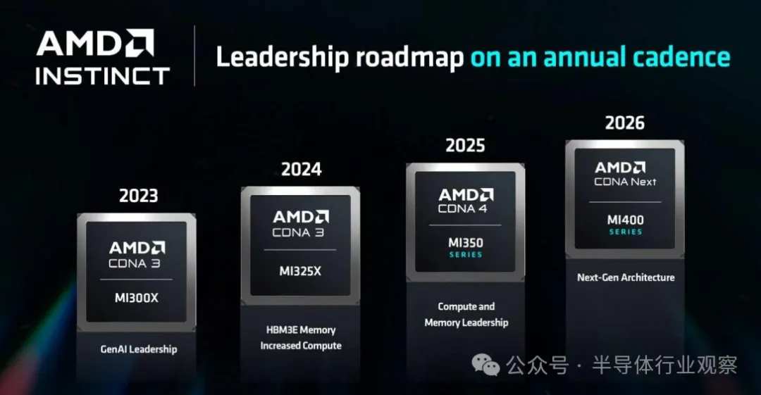
Following Nvidia, AMD also unveiled its AMD Instinct accelerator roadmap for an annual pace, introducing a new generation of AI accelerators each year. Lisa Su said, "Artificial intelligence is our top priority and we're at the beginning of an incredibly exciting time in this industry."
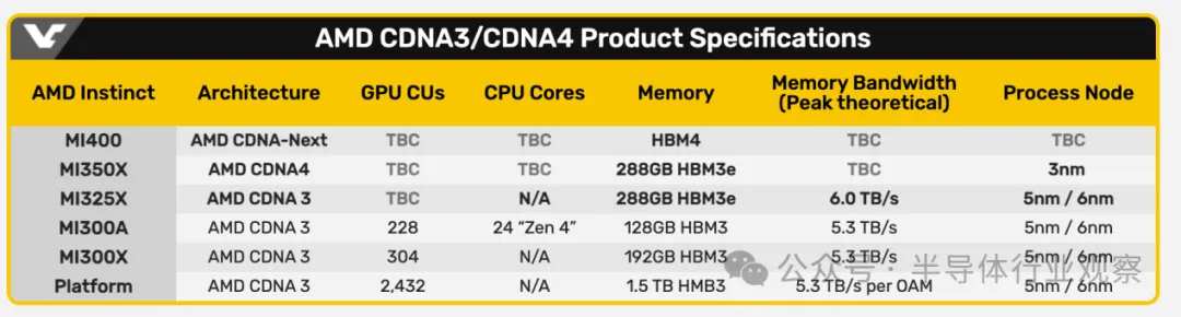
After launching the MI300X last year, AMD's next-generation MI325X accelerator will be launched in the fourth quarter of this year. The Instinct MI325X AI accelerator can be seen as a strengthened version of the MI300X series, which Lisa Su said has faster speed and larger memory. Then, the MI350 series will make its debut in 2025, using the new AMD CDNA 4 architecture. It is expected that compared with the AMD Instinct MI300 series with AMD CDNA 3, AI reasoning performance will be improved by 35%. The MI350 is benchmarked against Nvidia's Blackwell GPU, and according to AMD's data, the MI350 series is expected to offer 50% more memory and 20% more computational TFLOPs than Nvidia's B200 product. The AMD Instinct MI400 series based on the AMD CDNA "Next" architecture is expected to be launched in 2026.
Although Intel has a relatively conservative strategy, it is winning through pricing, and has taken an active pricing strategy with its Gaudi AI accelerator. Intel said that a standard data center AI suite consisting of eight Intel Gaudi 2 accelerators and one general-purpose board will be provided to system providers for $65,000, about one third of the price of a similar competing platform. Intel said that a suite containing eight Intel Gaudi 3 accelerators will be sold for $125,000, about two-thirds the price of a similar competing platform. Although AMD and Nvidia do not openly discuss the pricing of their chips, according to custom server supplier Thinkmate, the cost of a similar HGX server system equipped with eight Nvidia H100 AI chips may exceed $300,000.
As the chip giants surge forward, the speed of new product releases and pricing highlights the fierce competition in the AI chip market, leaving many AI startups behind. It is foreseeable that the three major chip giants will share most of the AI market, and a large number of AI startups will get only a small piece of the pie.
The process is moving towards 3 nanometers.
The trend of AI chips going towards 3 nanometers is inevitable, including data centers, edge AI, and terminals. Three nanometers is the most advanced process node currently, and the performance improvement, power consumption reduction and transistor density increase brought by the 3 nanometer process are important driving forces for the development of AI chips. For high-energy-consuming data centers, the low-power characteristics of the 3 nanometer process are critical. It can effectively reduce the operating costs of data centers, ease the energy pressure of data centers, and provide important support for the construction of green data centers.
Nvidia's B200 GPU has a power consumption as high as 1000W, and the GB200 solution consisting of two B200 GPUs and one Grace CPU consumes as much as 2700W of power. Such power consumption makes it difficult for data centers to provide power and cooling for large clusters of these compute GPUs, so Nvidia must take measures.
One of the design goals of the Rubin GPU is to control power consumption. Guo Mingchi, an analyst at TF International Securities, wrote on X that the Rubin GPU is likely to be manufactured using TSMC's 3-nanometer process technology. According to foreign media, the Rubin GPU will use a 4x photomask design and TSMC's CoWoS-L packaging technology. Whether the Rubin GPU can really reduce power consumption compared to Blackwell-based products while significantly improving performance or whether it will focus on performance efficiency remains to be seen.
The AMD Instinct series has been using 5nm/6nm dual-node Chiplet mode, and the MI350 series has also upgraded to 3nm. Semiconductor analyst Lu Xingzhi said that if NVIDIA has a large demand for TSMC orders under acceleration, AMD may not get enough production capacity and may turn to Samsung to place orders.
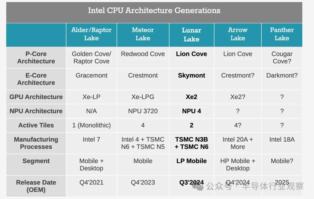
Intel's flagship chip Gaudi 3 for generative AI uses TSMC's 5nm process. For Gaudi 3, this part of the competition is slightly shrinking. However, Intel's focus seems to be more on AI PC. As can be seen from Intel's latest PC-side Lunar Lake SoC, it has also used 3nm. Lunar Lake includes a new Lion Cove P core design with the code name Lion Cove and a new wave of Skymont E cores, which replace the Meteor Lake Low Power Island Cresmont E cores. Intel has disclosed that it uses a 4P+4E (8-core) design and disables hyper-threading/SMT. The entire computing block, including the P core and the E core, is built on TSMC's N3B node, while the SoC block is manufactured using TSMC's N6 node.
In the field of edge and terminal AI chips, IP giant Arm also released the fifth-generation Cortex-X core for smartphones and a computing subsystem (CSS) with the latest high-performance graphics unit in May this year. The Arm Cortex-X925 CPU uses the 3nm process node, and thanks to this, the single-threaded performance of the CPU has been improved by 36%, and the AI performance has been improved by 41%, which can significantly improve the response capability of device-side generative AI, such as large language models (LLM).
High-bandwidth memory (HBM) is a necessity.
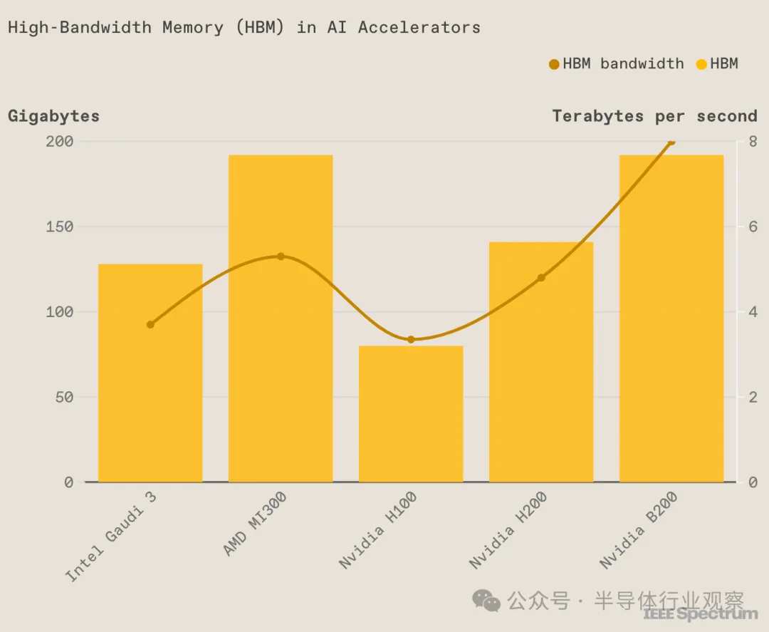
High-bandwidth memory (HBM) has become an essential key component for AI chips. HBM technology has gone through several generations of development: the first generation (HBM), the second generation (HBM2), the third generation (HBM2E), the fourth generation (HBM3), and the fifth generation (HBM3E), and is currently actively developing the sixth generation of HBM. HBM keeps breaking performance limits to meet the growing bandwidth demands of AI chips.
In the current generation of AI chips, almost all of them have adopted the fifth-generation HBM-HBM3E. For example, NVIDIA's Blackwell Ultra has increased its HBM3E to 12, and AMD's MI325X has 288GB of HBM3e memory, which is 96GB more than the MI300X. Intel's Gaudi 3 is packaged with eight HBM chips, and its ability to work together may be due in part to its use of cheaper HBM2e.
As for the next generation of AI chips, almost all of them have embraced the sixth generation of HBM-HBM4. NVIDIA's Rubin platform will be upgraded to HBM4, with 8 built-in HBM4 in Rubin GPU, and Rubin Ultra to be launched in 2027 with 12 HBM4. AMD's MI400 is also moving towards HBM4.
From the perspective of HBM suppliers, AMD, NVIDIA, and other major suppliers have previously mainly used SK Hynix. But now Samsung is also actively entering these manufacturers' internal systems, and both AMD and Samsung are currently testing Samsung's HBM. On June 4, at a press conference held at the Taipei Nangang Exhibition Center, Huang Renxun answered the question of when Samsung could become a partner of NVIDIA. He said, "We need a very large number of HBMs, so the speed of supply is crucial. We are working with Samsung, SK Hynix, and Micron, and we will receive products from these three companies."
The competition for HBM is also very intense. SK Hynix initially planned to mass-produce HBM4 in 2026, but has now adjusted its schedule to an earlier date. Samsung Electronics has also announced plans to develop HBM4 next year. Competition between Samsung and SK Hynix for HBM is also fierce, with both companies shifting 20% of their DRAM production capacity to HBM this year. Micron has also joined the battle for HBM.
HBM, which is in high demand, has become a bottleneck for large-scale production of AI chips. Currently, SK Hynix's HBM4 production capacity until 2025 has been almost sold out, and the supply-demand contradiction is becoming increasingly prominent. According to SK Hynix's forecast, the prosperity of the AI chip market will drive the HBM market to a compound annual growth rate of 82% by 2027. Analysts also believe that the HBM market is expected to grow more than twice this year.
Hwang Sang-joon, executive vice president of Samsung Electronics' DRAM products and technology, said at the KIW 2023: "Our customers' current (HBM) order decisions have increased by more than double last year." Kyung Kye-hyun, president of Samsung's equipment solutions division responsible for chip business, also said at the company meeting that Samsung will strive to take more than half of the HBM market. Jaejune Kim, executive vice president of Samsung's memory business, told analysts that the company plans to double its HBM production capacity between 2023 and 2024.
Interconnectivity: an important puzzle piece.
Interconnectivity between AI chips has always been a problem. As more and more accelerators are integrated together, how to efficiently transmit data has become a bottleneck. Because the development speed of PCIe technology cannot keep up with the demand of the times, mainstream AI chip manufacturers have developed their own interconnect technologies, among which NVIDIA's NVLink and AMD's Infinity Fabric are more representative.
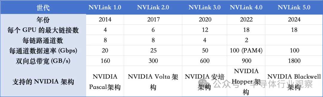
NVIDIA's next-generation Rubin platform will use NVLink 6 switch chips with a running speed of 3,600GB/s, while the previous generation's Blackwell used NVLink 5.0. NVLink was designed to address the bandwidth limitations of traditional PCI Express (PCIe) buses in handling high-performance computing tasks. The following figure shows the parameter situation of NVIDIA's generations of NVLink.
Similar to NVIDIA's NVLink, AMD has launched its Infinity Fabric technology. The AMD Infinity architecture was launched together with the second-generation AMD EPYC processors, allowing system builders and cloud architects to unleash the latest server performance while not sacrificing functionality, manageability, or the ability to protect their organization's most critical assets (data). Infinity Fabric supports data transfer between chips, chip pairs, and upcoming node-to-node.
Intel is a staunch supporter of Ethernet, and its Gaudi AI chip for generative AI continues to use traditional Ethernet interconnection technology. Gaudi 2 uses 24 100Gb Ethernet links per chip; Gaudi 3 also uses 24 200Gbps Ethernet RDMA NICs, but doubles the bandwidth of these links to 200Gb/s, making the external Ethernet I/O total bandwidth of the chip reach 8.4TB/s.
Service-oriented
Complex generative AI development tasks like ChatGPT require large models to run billions to tens of trillions of parameters across multiple computers in parallel, using various parallel processing methods such as tensor parallelism, pipeline parallelism, and data parallelism, to process tasks as quickly as possible.
Therefore, how to help users develop faster and provide good service is also a key factor.
In this regard, NVIDIA has introduced a new software called NIMS, which stands for NVIDIA Inference Microservices. Huang Renxun calls it "AI in a box." NIMS contains NVIDIA's CUDA, cuDNN, TensorRT, and Triton. NIMS not only makes AI deployment easier, taking only minutes instead of months, but also makes them building blocks for customers to create new applications and solve new problems. If used, NIMS will help accelerate innovation and shorten the time to value realization. Nvidia also announced that NIMS is now available for free use by developers and researchers. Deploying NIMS in production requires an AI Enterprise license, at a price of $4,500 per GPU.
Conclusion
The next AI battle has begun. Overall, in the current AI chip market, major chip giants such as NVIDIA, AMD, and Intel are engaged in fierce competition. They are not only competing in speed, technology, and process innovation but also actively expanding their interconnection and service capabilities to provide faster, stronger, and smarter AI solutions to users. The AI chip battle is still ongoing, and let's wait and see who will eventually win.
Editor/Lambor