
Launching direct drawing equipment "Ledia Qs" for package substrates.
SCREEN PE Solutions recently developed a high-resolution model of the direct drawing equipment "Ledia Qs" for package substrates and will start selling it from June 2024.
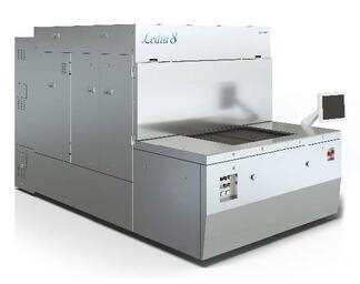
Ledia Qs
The print data of this image (resolution 300dpi) can be downloaded from the following URL:
In recent years, with the spread of 5G and IoT infrastructure and the progress of new technology areas such as generative AI, demand for semiconductor devices has been expanding on a global scale, especially for high-end substrates such as package substrates that mount semiconductor devices in the printed circuit board industry. Investments are expected to continue in this field in the future.
In the past, stepper adoption had been progressing for the solder resist exposure process for high-end substrates, but direct drawing equipment had been eagerly anticipated due to higher positional accuracy requirements, resolution, and convenience, among other factors.
In response to these industry needs, we have developed the latest model of the "Ledia series," the "Ledia Qs." This equipment is based on our company's own exposure head, which boasts the highest resolution in the industry as a broadband wavelength type exposure equipment, and integrates the technology developed last year for "Ledia 8F," achieving high drawing quality and stable drawing positional accuracy.
By expanding the lineup of the "Ledia series" this time, we will accelerate our business in the growing printed circuit board market and continue to respond to various needs in the electronic equipment industry, contributing to the development of the industry.