
Recently, well-known analyst Guo Mingyi revealed information about Nvidia's next generation AI chip R series/R100 AI chip. According to him, the chip will enter mass production in the 4th quarter of 2025, and mass production of the system/rack solution is likely to begin in 2026 1H20.
In terms of process, the R100 will use TSMC's N3 process (vs. B100 using TSMC's N4P) and Cowos-L package (same as B100). Meanwhile, the R100 uses approximately 4x reticle design (vs. B100's 3.3x reticle design).
When it comes to the size of the Interposer, according to Guo Mingqi, Nvidia has not yet finalized the bill, but there will be 2-3 options.
As for the much-publicized HBM, the R100 is expected to be equipped with 8 HBM4s.
Meanwhile, Nvidia's GR200 Grace CPU will use TSMC's N3 process (vs. GH200/GB200 CPUs use TSMC N5).
According to Guo Mingqi, Nvidia has understood that the energy consumption of AI servers has become a challenge in CSP/Hyperscale procurement and data center construction. Therefore, in addition to improving AI computing power, improving energy consumption is also a design focus of the R series chip and system solutions.
Nvidia's chip roadmap, in-depth interpretation
In October 2023, Nvidia updated its latest data center roadmap, and its aggressive update range updated everyone. First, let's review Nvidia's roadmap over the past few years. Here's what was announced at GTC 2021 in April 2021:
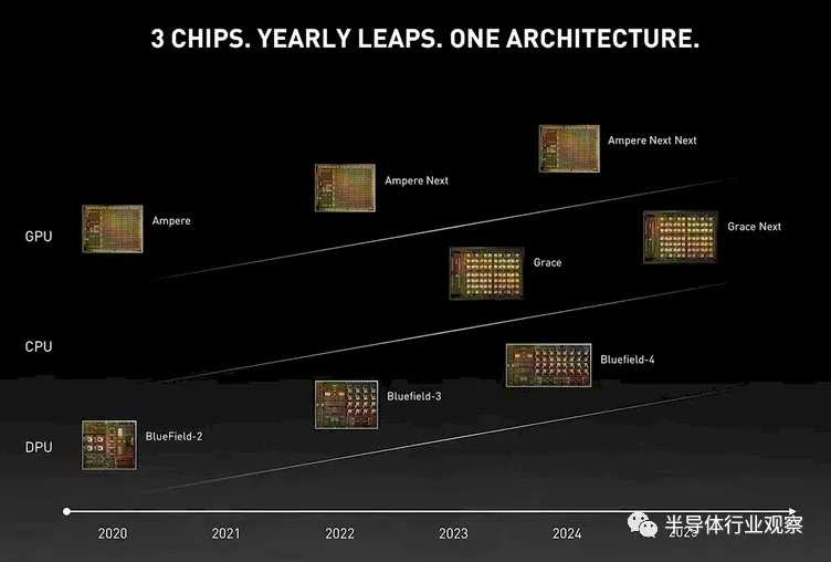
This is an updated version after “Hopper,” called “Ampere Next” in the roadmap above, and released at Computex in 2022:
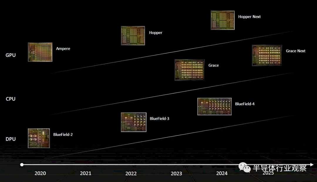
Here's an update to the roadmap we think was released earlier this year, adding the “Lovelace” GPU family for artificial intelligence inference, visualization, and metaverse processing cards:

Finally, this is the roadmap recently released by Nvidia, which was first revealed by semianalysis.

If past trends are indicators of future trends — when chipmakers promise their hyperscale and cloud builder customers a biennial launch pace, they should definitely be indicators of future trends, just like Nvidia did a few years ago — then we definitely expect the newly architected Blackwell GB100 GPU accelerator to launch around March to May next year. But as you can see below, the pace at which Nvidia's main GPUs are released is usually less than two years old. So it's a form of regression.
Here's how data center GPUs have been introduced over the past 21 years. Data center GPU computing is critical:
“Kepler” K10 and K20, May 2012
“Kepler” K40, May 2013
“Kepler” K80, two GK210B GPUs on a single card
“Maxwell” M40, November 2015, mainly used for AI inference, not really for HPC or AI training
“Pascal” GP100, April 2016
“Volta” GV100, May 2017 (some features of the original Pascal didn't appear until Volta)
“Ampere” GA100, May 2020
“Hopper” GH100, March 2022
“Hopper-Next” H200, spring 2024?
“Blackwell” GB100, summer or fall 2024?
“Xavier” GX100, spring/summer 2025
We know very well that Hopper-Next should be a Blackwell GB100 GPU, and the GH200 on the roadmap now is a stopgap to try to divert attention from AMD's CPU-GPU hybrid devices “Antares” Instinct MI300X GPU and MI300A hybrid graphics cards that look like it will launch in December. AMD will have the advantages of HBM memory capacity and bandwidth on these devices, as well as aggregate memory for the CPU and GPU, and Nvidia can't tell everyone that the H100NVL double card is the answer.
So there are two ways to use the upcoming Hopper-Next H200 GPU. The one we agree with, but only based on a hunch, is that Nvidia tests put two Hopper GH100 GPUs in one slot, as it already uses its Arm server CPU to work with its Grace-Grace superchip. We suggested it do this a year and a half ago. The chip's performance can be slightly reduced to obtain a more suitable power range and leave room for higher HBM3e memory stacks, thereby increasing the memory-to-compute ratio, which is currently very scarce in data centers.
The number of chips in a GPU slot isn't as important as the bandwidth in each slot. Each slot requires two GPUs, but four, six, or eight times the memory bandwidth is required to really get ahead and improve the GPU's performance. We're half-joking: it might make more sense to have half a Hopper GPU — call it Hop? — If you really want to improve the performance of your AI workloads, you need 2x the memory capacity and 2x the memory bandwidth.
Some people think the H200 is just a memory upgrade, providing 2x the memory capacity and 2x the memory bandwidth on the same GH100 GPU. We think it will be tweaked a bit, and maybe a deeper level of garbage sorting to at least improve performance.
There's another annoying thing in this roadmap: According to Nvidia's latest roadmap, when exactly will the future Blackwell GB100 GPU and B100 accelerator appear? Do you see the date on it? We're guessing it's late 2024, but Blackwell still has some room to delay until early 2025. (We think the Blackwell chip is probably named after Elizabeth Blackwell (Elizabeth Blackwell), the first woman to obtain a medical degree in the US (Geneva Medical School in upstate New York, now part of Syracuse University), and the first woman to be registered on the British General Medical Council medical register.)
In any case, the Blackwell GB100 GPU is very close to the GX100 GPU (we codename it “Xavier”) and is expected to launch in 2025, which we think will be later this year, but probably not. (Other than the fictional Charles Xavier in the Marvel superhero universe, we can't find any significant famous scientist whose last name ends with X; yes, we know Nvidia already uses that codename in one of its embedded systems. “X” probably just means it's a variable, and Nvidia hasn't decided on a codename yet.)
We think Nvidia needs more time to adjust Blackwell's GPU architecture, and considering how fast the AI model is changing, if things matter, such as Volta's Tensor Cores or sparseness, Nvidia should be reasonable and the right support is for Ampere, or the Transformation Engine and FP8 for Hopper.
Once this is fixed, we have a few things to pick on the current Nvidia roadmap. For instance, what happened to the BlueField DPU?
DPUs are an integral part of Nvidia's hardware stack, providing networking, security, and virtualization offload, and turning supercomputers into multi-tenant clouds. The Hopper GPU was announced at the March 2022 Spring GTC conference, not in 2023, and was also shipped in late 2022. The H100 NVL and Lovelace L40 are missing. The “Ampere” A100 came out in 2020, not 2021. Quantum 2 400 Gb/s InfiniBand and 400 Gb/s Spectrum-3 Ethernet were released in 2021, and shipments began in 2022 (not 2023). 800 Gb/s Ethernet and InfiniBand are running about a year later than we expected when we spoke with Nvidia in November 2020. Incidentally, the previous generation 200 Gb/s Quantum InfiniBand was released in 2016 and shipped in 2017. There's a big gap there, because all companies trying to market the jump from 200 Gb/s to 400 Gb/s have this gap.
In light of all this, we've updated the official Nvidia roadmap:

Clearly, the explosive growth of generative artificial intelligence has eliminated the hesitation of data centers and supercomputing executives about computing and interconnection. Therefore, the once-a-year rhythm makes sense. However, without some slippage, it may be difficult to maintain. In fact, this roadmap can be seen as a way to make up for delays in the delivery of the Blackwell architecture, and the fact that the Xavier GX100 will launch in 2025 (probably very close to Blackwell) tells you that something has already happened. Maybe Nvidia will start with Blackwell and move to launch and deliver its data center GPUs in the fall? No matter what the H200 GPU accelerator is, it's worth noting that no B200 or X200 comes close behind. This H200 is a little horse that only plays tricks.
Here are a few things to consider: When demand for a product is 3x, 4x, or even 5x what you can deliver, the pace of the roadmap doesn't matter; supply matters more. What if the cloud and some artificial intelligence startups get all the Hopper GPUs and no one else can? That means anyone with a matrix math engine and artificial intelligence framework has the chance to sell whatever they get.
So we're seeing this happening, even with dead-end products like Intel's highly regarded Gaudi accelerator series. Yes, Gaudi 2 can compete with Nvidia A100 or even H100, yes, Gaudi 3 is coming soon and will double its performance, but so what? There is no Gaudi 4, but there is a GPU called “Falcon Shores,” which has Gaudi matrix math units and Gaudi Ethernet interconnect. Under normal circumstances, no one would buy a Gaudi 2. But in the generative AI gold rush, any matrix math unit you can get must do that.
After taking a close look at this road map, this is probably the most important thing. Nvidia has plenty of cash to monopolize the HBM memory and CoWoS substrate market, and is far ahead of competitors who also need these components to build accelerators. It can use upcoming components, such as TSMC's very interesting CoWoS-L packaging technology, which allows relatively normal substrate packaging of small chips, but places a small intermediate layer between the small chips, and requires a large number of wires to drive high voltages. Bandwidth between parts of these small chips. (CoWoS-L is a bit like Intel's EMIB.) It has enough cash to make a two-chip H200 and a four-chip B100 if it wants to. Nvidia has proven the viability of the four-GPU design, but to be fair, the MI300X shows that AMD can do this by stacking eight small chips on top of a huge L3 cache.
Nvidia is better off not messing around, because when it comes to hardware, AMD definitely won't. Those who love open source frameworks and models are closely watching the PyTorch 2.0 framework and the LLAMA 2 large language model, which have no barriers due to Meta's enlightened egoism. PyTorch clearly works great on AMD processors, and we think it would do better on the MI300A and MI300X.
So starting in 2024, the pace of Nvidia chips has really accelerated the pace of upgrades every year.
Remember, you can build a moat, but you can't drink it when the well dries up because the water is stinky and probably comes from enemy corpses
Finally, let's review what semianalysis said at the time.
B100, time-to-market is above everything else
We believe Nvidia's B100 will be shipped in large quantities in the third quarter of 2024, with some early samples available in the second quarter of 2024. Judging from the performance and total cost of ownership we've heard, it beats Amazon Trainium 2, Google TPUv5, AMD MI300X, Intel Gaudi 3, and Microsoft Athena, even considering the much lower profits paid to buy these chips from design partners/AMD/TSMC.
We understand that compared to the original “plan,” Nvidia made a number of compromises to bring the B100 to market faster. For example, Nvidia wanted to set the power consumption to a higher level of 1,000W, but they would initially stick with the H100's 700W. This allowed Nvidia to stick with air cooling when the B100 variant went on sale.
Nvidia also initially insisted on PCIe 5.0 on the B100. The combination of 5.0 and 700W means it can be plugged directly into the H100's existing HGX server, greatly increasing the supply chain's ability to increase production and shipments earlier in the supply chain. Part of the reason for the decision to stick with 5.0 is that AMD and Intel are far behind in PCIe 6.0 integration. Nvidia's own internal team isn't ready to use PCIe 6.0 CPUs, plus they'll use faster C2C-style links.
ConnectX-8 was later equipped with an integrated PCIe 6.0 switch, but no one was ready for it yet. Our understanding is that Broadcom and Astera Labs will only be ready to ship PCIe 6.0 retimers in bulk by the end of this year, and given the size of these substrates, many retimers are still needed. This means that the original B100 will be limited to 3.2T, while the ConnectX-7 will be limited to 400G instead of 800G per GPU as Nvidia Slides claims. Keep the air cooling, power, PCIe, and network speeds the same, making it extremely easy to manufacture/deploy.
Nvidia will launch a 1000W version later, which requires water cooling. This variant appeared a little later, and will enable full 800G per GPU network via ConnectX-8. These SerDes are still 8x100G for Ethernet/InfiniBand. Although the network speed of each GPU doubled, the base figure was halved because they still had to go through the same 51.2T switch. There will be no 102.4T switches in the B100 generation.
Interestingly, we've heard that Nvidia is moving to the 224G SerDes NVLink component on the B100, and it would be great if they could make it work. Most people we've talked to think 224G is unreliable and unlikely to happen in 2024, except for those at Nvidia. We don't know, but they're likely to stick with 112G in 2024, but we're currently leaning towards Nvidia taking an aggressive approach. Note that Google, Meta, and Amazon own 224G AI accelerators and target mass production over 2026/2027, rather than 2024/2025 like Nvidia. Nvidia will beat their rivals.
We've heard that this GPU is still TSMC's N4P, not based on 3nm process technology. This makes sense considering TSMC's 3nm is immature for such a large chip size. Based on the rumored substrate size from its substrate supplier Ibiden, Nvidia appears to have switched to 2 single-chip large chip MCMs with 8 or 12 HBM stacks. This is a macro design similar to SambaNova and Intel's next year's chips.

Nvidia doesn't use any crazy hybrid bonding like AMD because they need to ship a very large capacity, and cost is a big issue for them. We believe these two B100 variants will have similar or more memory capacity and more memory bandwidth to the MI300X. The air-cooled B100 can have a 6.4Gbps stack, but the water-cooled version can be as high as 9.2Gbps.
Nvidia also showcased the GB200 and B40. G stands for GB200 and GX200, so it's clearly a placeholder as Nvidia will launch new Arm-based CPUs. They won't be using Grace for this long. We think the B40 is half of the B100, with just 1 monolithic N4P chip and up to 4 or 6 HBM stacks. Unlike the L40S, this makes sense for inference with smaller models.
X100, a fatal blow
Most notable is Nvidia's “X100” schedule. This schedule will match AMD's current MI400 schedule. AMD's MI300X strategy is to launch one year after the H100. AMD hopes that by being technologically aggressive, the MI300X fills an impressive package with more compute and memory, and can surpass Nvidia in pure hardware compared to the H100 a year ago.
Nvidia found that their 2-year data center GPU product pace could open a window for competitors trying to gain a foothold in the market with newer chips. Now, Nvidia is closing that window by speeding up the product pace to once a year. The “X100” is expected to launch in 2025, just one year after the B100.
Given that this GPU is still far from streaming, unlike the B100, the B100 has already been taped out, and things are still unresolved. Nvidia has never discussed issues after the next generation, so this is unprecedented.
The name is clearly not “X100” either. Nvidia has always codenamed their GPUs after prominent female scientists such as Ada Lovelace, Grace Hopper, and Elizabeth Blackwell. For X, the only logical person is Xie Xide, a Chinese female scientist who studies the structure of semiconductors and metal energy bands. However, we highly doubt this, although this may be how Nvidia plans to sell GPUs to China again after rumored export restrictions next week.
Jokes aside, this “specification” isn't worth guessing about, because the netlist isn't even complete. The only intersection is the use of TSMC's N3X.
Editor/Jeffrey