
Source: Core Stuff
A single core doesn't matter; what really matters is solving the challenge of improving system-level performance and energy efficiency. Compared to the previous generation Hopper, the main optimization of Blackwell GPUs does not rely on improvements in process technology, but rather more advanced memory, faster on-chip interconnect speed, and expandability, and management software to eliminate communication bottlenecks caused by massive data processing, thus connecting a large number of GPUs into a more cost-effective and powerful system.
Xinxi reported on March 24 that the two most expensive Chinese in the world today, one sells shovels and the other sells water.
The first place is Nvidia's founder and CEO Huang Renxun, who sold GPUs to AI gold diggers and promoted Nvidia to the third largest market capitalization in the world; the other was Zhong Yuyi, founder, chairman, and general manager of Nongfu Spring, who is proud to be a “natural carrier” for drinking water.

Currently, Nvidia's market capitalization has settled at the 2 trillion US dollar mark, and the market capitalization gap with Apple has narrowed to 0.3 trillion US dollars.

At the Nvidia GTC conference this week, Hwang In-hoon seriously said, “We can sell hot water with it.”
This is no joke. Hwang In-hoon is based on data: the liquid cooling and cooling of the new Nvidia DGX machine is 25℃, close to room temperature; the outlet temperature rises to 45℃, close to the water temperature of the jacuzzi, and the flow rate is 2 L/s.
Of course, compared to selling water, GPU computing power is Nvidia's banknote printer.
Hwang In-hoon, known as the “Leather Swordsman,” has always had a strong sense of crisis and risk, and is always paving the way for the future ahead of schedule. In addition, the chip industry is a high-risk, high-cost, and low-fault tolerant industry. If you take one wrong step, you may fall to the bottom of the world, and you will lose everything. Therefore, at a critical moment when demand for AI computing power is exploding like never before, Nvidia is afraid to slack off the slightest bit on new products; it will inevitably have the biggest explosion in the short term, leaving rivals out of reach.
While competitors are still aiming to catch up with Nvidia's flagship GPUs, Hwang In-hoon is already at the next level, capturing the pain point of data center customer needs — a single core is not enough; what really matters is solving the challenge of improving system-level performance and energy efficiency.

Compared to a single flagship GPU, Nvidia's chip is indeed worthy of the “nuclear bomb” title. It has excellent performance and high power consumption. However, Hwang In-hoon has long since broken out of the chip itself and continues to instill in data center customers the concept of “buy more, save more”. Simply put, buying Nvidia's AI system solution is faster and cheaper than other solutions.
From Blackwell's architecture design to the technical layout of AI infrastructure, it can reflect Huang Renxun's forward-looking judgment on future market needs and industry trends:
1. Moore's Law drives performance improvements to the limit. The single die area and transistor are fast to the limit. Subsequent chip iterations must include innovative combinations of technologies such as high-bandwidth memory, advanced Chiplet packaging, and on-chip interconnection. Coupled with the optimization of high-performance communication such as off-chip interconnection, it forms the foundation for Nvidia to create a system specially designed for trillion parameter-level generative AI.
2. In the future, data centers will be viewed as AI factories. Throughout the life cycle, the goal of AI factories is to generate revenue. Unlike the consumer market where video cards are sold separately, the data center market is a system-level business. The peak performance of a single chip has little reference value. Combining many GPUs into one “giant GPU” makes it consume less cards, time, and electricity to complete the same computing tasks, making it more attractive to customers.
3. The scale and data volume of AI models will continue to grow: in the future, multi-modal data will be used to train larger models; world models will become popular, learning to grasp the physical laws and common sense of the real world; with synthetic data generation technology, AI can even mimic the way humans learn, associate, think, and train each other. Nvidia's goal is to continuously reduce computing-related costs and energy consumption.
4. High-performance inference or generation will be critical. Nvidia GPUs running in the cloud are probably used for token generation for half of the time, running a large number of generative AI tasks. This requires not only increasing throughput to reduce service costs, but also increasing interaction speed to improve user experience. One GPU is not up to the task, so it is necessary to find a method that can process models in parallel on many GPUs.
01 Detailed explanation of the strongest AI chip specifications: maximum power consumption is 2700W, CUDA configuration is a mystery
On Tuesday, Nvidia released a new generation of Blackwell GPU architectures, which not only deliberately weakens the presence of a single chip, but also does not specify the GPU code name, but is also vaguely called a “Blackwell GPU.” This somewhat added a hint of mystery to Blackwell's architecture, which is recognized as being far ahead.
At the GTC conference site, Nvidia Vice President Ian Buck and Senior Vice President Jonah Alben further shared their thoughts behind Blackwell's architectural design with global media such as Smart Electronics & Silicon West. In conjunction with the 22-page Nvidia Blackwell architecture technical brief, configuration details on the GB200 superchip, HGX B200/B100, DGX supercomputer, etc. were further disclosed.
According to available information, the new Blackwell GPU does not use the most advanced 3nm process, but instead continues to use the 4nm custom enhanced process TSMC 4nP. There are 3 types of known chip models — B100, B200, and GB200 superchips.
The B100 is not the protagonist of the new release; it is only mentioned in the HGX B100 board. The B200 is the highlight, and the GB200 further combines the B200 with a 72-core Grace CPU.
The B200 has 208 billion transistors, more than double the number of H100 (80 billion transistors). Nvidia did not disclose the exact size of a single Blackwell GPU die, only that it is within the reticle size limit. The previous generation single die had an area of 814 mm². Since I don't know the exact figures, it is difficult to calculate the extent of improvement in B200's performance per unit area.

Through the NV-HBI high-bandwidth interface, Nvidia packages the two GPUs die with 10Tb/s bidirectional bandwidth, so that the B200 can operate as a single chip without loss of performance due to communication loss, no memory locality issues, and no caching issues, and can support higher L2 cache bandwidth. However, Nvidia did not disclose exactly what kind of chip packaging strategy it adopted.
The previous GH200 superchip was a combination of 1 H100 and 1 Grace CPU. The GB200 superchip combines 2 Blackwell GPUs and CPUs, and the full TDP of each GPU reaches 1200W, making the TDP of the entire superchip reach 2,700W (1200W x 2+300W).

It is worth noting that the Blackwell architecture technical brief only revealed Tensor core data, and did not mention any information such as the number of CUDA cores, number of Tensor cores, and vector computing power. With the exception of FP64, which is dense, all other data formats show sparse computing power.
In contrast, the standard FP64 Tensor core computing performance has not improved much. The H100 and H200 are 67 TFLOPS, and the GB200 superchip is 90 TFLOPS, an increase of 34% over the previous generation.
One possible guess is that the design of the Blackwell architecture is completely biased towards AI computing, and the improvement in high-performance computing is not obvious. If the transistors are all used in the stack Tensor core, its general capability will be weakened, more like a partial AI NPU.
Because of the same infrastructure design, switching from Hopper to a Blackwell motherboard is as easy as a sliding drawer.
The technical brief revealed the system configurations of Blackwell x86 platforms HGX B100 and HGX B200. The HGX B200 is equipped with 8 B200s, and the TDP of each GPU is 1000W; the HGX B100 is equipped with 8 B100s, and the TDP of each GPU is 700W.

After the launch of the Blackwell GPU in the data center, the industry's focus shifted to the RTX 50 series gaming graphics card, which is also based on the Blackwell architecture. Currently, the RTX 50 series GPUs are still far from the release date, and they can be obtained as soon as the end of this year; the slower pace may be until next year or even the year after.
However, there are many rumors about the configuration. For example, using TSMC's 3nm and 28Gbps GDDR 7 video memory, the maximum bus width is 384 bits and 512 bits. The chip includes everything from the entry-level GB207 to the high-end GB202, and will continue to optimize path tracking and light tracking.
02 How did Nvidia achieve a 1,000 times increase in AI training computing power in 2008?
From the 19TFLOPS of the 2016 Pascal GPU to the 20PFLOPS of this year's Blackwell GPU, Hwang In-hoon announced that Nvidia has increased single-card AI training performance by 1000 times in 8 years.

In addition to benefiting from process iterations, greater HBM capacity and bandwidth, and dual-die design, this sounded exciting multiple.

Most training is performed with FP16 accuracy, but in reality, there is no need to process all parameters with this high accuracy. Nvidia has been exploring how to use mixed-precision operations to reduce memory usage while ensuring that throughput is not affected.
The second-generation Transformer engine built into Blackwell GPUs uses advanced dynamic range management algorithms and fine-grained scaling technology (micro-tensor scaling) to optimize performance and accuracy, and supports the new FP4 format for the first time, doubling the FP4 Tensor core performance, HBM model size, and bandwidth.

At the same time, TensorRT-LLM's innovations include a customized kernel with quantization to 4 bit accuracy and expert parallel mapping, which allows real-time inference of MoE models to consume hardware, energy, and costs. The NeMo framework and Megatron-Core's new expert parallel technology all support the improvement of model training performance.
The difficulty of reducing accuracy is taking into account the user's need for accuracy. FP4 doesn't work all the time; Nvidia specifically emphasizes the benefits of mixing expert models and big language models. Reducing the accuracy to FP4 may increase the level of confusion. Nvidia has also thoughtfully added a transition FP6. Although this new format has no performance advantage, the amount of data processed is reduced by 25% compared to FP8, which can reduce memory pressure.
03 In 90 days, 2,000 GPUs train a 1.8 trillion parameter model, breaking communication bottlenecks is the key
Unlike the consumer-grade video card strategy, for data centers, Huang Renxun does not plan to make a small profit by selling one or two video cards, but instead takes the “storage” route to help customers save money.
Whether it's greatly improving performance, saving rack space, and reducing electricity costs, they are all very attractive to companies racing against time in the AI big model competition.
The example given by Hwang In-hoon is a GPT-MoE hybrid expert model that trains 1.8 trillion parameters:
Using 25,000 Ampere GPUs, it takes about 3 to 5 months; if you use Hopper, it takes about 8,000 GPUs and 90 days to train, and consumes 15 MW of electricity; using Blackwell, it also takes 90 days, only 2,000 GPUs, and consumes only 4 MW of electricity.
Saving money is directly proportional to saving electricity; the key to improving energy efficiency is to reduce communication losses. According to Ian Buck and Jonah Alben, running a huge GPT-Moe model on a GPU cluster spends 60% of the time communicating.

Ian Buck explains that this is not just a computational problem, but an I/O problem; the mixed expert model brings more layers of parallelism and communication. It breaks down the model into groups of experts who are good at different tasks. Whoever is good at what is assigned the corresponding training and reasoning tasks.

Therefore, it is important to implement faster NVLink Switch interconnect technology. All GPUs must share the results of the calculation process. In the DGX GB200 NVL72 frame, multi-node all-to-all communication and all-reduce communication speeds have skyrocketed compared to the past.

The total bandwidth of the new NVLink Switch chip reaches 7.2Tb/s, supports vertical GPU expansion, and can drive 4 1.8TB/s NVLink ports. PCIe 9.0 x16 slots are not expected to provide 2Tb/s of bandwidth until 2032.
Looking at a single card, compared to the H100, the training performance of the Blackwell GPU was only increased 2.5 times, and even based on the newly added FP4 accuracy, the inference performance was only increased by 5 times.
However, if we look at system performance, compared to the previous generation Hopper cluster, Blackwell can increase GPT-MoE inference performance with 1.8 trillion parameters by 30 times.

The blue curve represents the H200, and the fuchsia curve represents the B200. Going from blue to purple only involves chip upgrades from Hopper's single-core design to Blackwell's dual-core design. Coupled with new technologies such as FP4, Tensor Core, Transformer Engine, and NVLink Switch, the performance has increased to the GB200 represented by the green curve.
In the figure below, the Y axis is the number of tokens per GPU per second, representing data center throughput; the x axis is the number of tokens per user per second, representing the user's interactive experience. The closer to the upper right, the data indicates that both capabilities are strong. The green curve is the peak performance line.

In order to find the correct parallel configuration for GPT-MoE training, Nvidia conducted numerous experiments (obtaining the blue points in the figure) to explore the correct method of creating hardware and cutting models to make them run as efficiently as possible. The exploration includes some software rechunking, optimization strategy judgment, and distributing large models across different GPUs to meet performance requirements.
TP2 on the left represents tensor parallelism across 2 GPUs, EP8 represents expert parallelism across 8 GPUs, and DP4 represents data parallelism across 4 GPUs. There is TP4 on the right. Tensor parallelism across 4 GPUs and expert parallelism across 16 GPUs. Different configurations and distribution strategies at the software level can cause different results at run time.
Huang Renxun also explained that the Blackwell DGX system can save more electricity and money from the perspective of communication consumables.
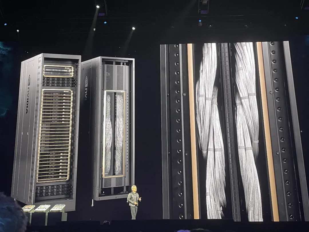
He explained that the NVLink backbone data on the back of the DGX uses 130Tb/s bidirectional bandwidth to pass through the back of the chassis, which is higher than the total bandwidth of the Internet. Basically, all content can be sent to everyone within 1 second. There are 5,000 NVLink copper cables with a total length of 2 miles.
If optical transmission is used, an optical module and retimer must be used. These two devices consume 20 kW of electricity, and the optical module alone consumes 2 kW of electricity. Just to drive the NVLink backbone, Nvidia can do it without power consumption through the NVLink Switch, and can also save 20kW for computing (the entire rack consumes 120kW).
04 Assemble high-speed communication capabilities to build an E-class computing power AI supercomputer on a single frame
A faster network brings more powerful computational efficiency.
The DGX GB200 NVL72 uses a liquid-cooled rack design. As the name suggests, 72 GPUs are interconnected via fifth-generation NVLink at a communication speed of 1.8 Tb/s. At most, a rack has up to 130Tb/s GPU bandwidth and 30TB of memory. The training computing power is close to E-level, and the inference computing power exceeds E-level.

Compared to systems with the same number of H100 GPUs, the GB200 NVL72 provides 4 times the training performance for language models such as GPT-MoE-1.8t. The GB200 NVL72 uses 32 Blackwell GPUs to run GPT-Moe-1.8T, which is 30 times faster than 64 Hopper GPUs.

Hwang In-hoon said that this is the world's first single-frame EFLOPS class machine, and there are only two or three E-class machines on the entire planet.
In contrast, 8 years ago, he handed over the first DGX-1 to OpenAI, and the training computing power was only 0.17 PFLOPS.
The total bandwidth of the fourth generation NVLink with the H100 was 900 GB/s, while the fifth generation doubled to 1.8 Tb/s, which is more than 14 times the bandwidth of PCle 5. The number of NVLinks per GPU has not changed; all are 18 links. The communication speed between the CPU and B200 is 300Gb/s, which is faster than the 256Gb/s of PCIe 6.0 x16 slots.

The GB200 NVL72 requires a powerful network for optimal performance, using Nvidia Quantum-X800 InfiniBand, Spectrum-X800 Ethernet, BlueField-3 DPU, and Magnum IO software.

Two years ago, the GPU that Hwang In-hoon saw was an HGX, which weighs 70 pounds and has 35,000 parts; now the GPU has 600,000 parts and weighs 3,000 pounds. “Not a single elephant should have sunk” and “weighs about the same as a carbon fiber Ferrari.”
The fifth-generation NVLink increased the expandable number of GPUs to 576. Nvidia is also introducing some AI security features to ensure maximum uptime of data center GPUs. Eight GB200 NVL72 racks can form a SuperPod, interconnect with 800Gb/s InfiniBand or Ethernet, or create a large shared memory system with 576 GPUs interconnected.

According to Ian Buck, the current maximum configuration of 576 GPU interconnects is mainly for research, not production.
05 Conclusion: Eight years of progress, one dynasty climbed to the top
From the perspective of building a vertical ecosystem, Nvidia is increasingly like Apple in the field of chips and AI computing, showing strong and comprehensive dominance in R&D, engineering, and ecology.
Just as Apple uses the App Store to firmly stick to developers and consumers, Nvidia has built a complete set of chips, systems, networks, security, and software needed by various developers, using the best combination of software and hardware to continuously lower the threshold for accelerating AI computation on GPUs, making it always in the top of the list of enterprises and developers.
In data centers, there is no point in looking at the peak performance of a single chip. Only substantial computational power improvements achieved by connecting many chips together are directly indicative. Therefore, Hwang In-hoon wants to sell the “system”, which is the end point of data center customer computing power requirements one step at a time.
Compared to the previous generation Hopper, the main optimization of Blackwell GPUs does not rely on improvements in process technology, but rather more advanced memory, faster on-chip interconnect speed, and expandability, and management software to eliminate communication bottlenecks caused by massive data processing, thus connecting a large number of GPUs into a more cost-effective and powerful system.
Grass snake grey line, thousands of miles long. Nvidia explored the path of system design that integrates various aspects such as chips, storage, networks, and software as early as 8 years ago. In April 2016, Hwang In-hoon personally gifted the OpenAI team with the first supercomputer DGX-1 with 8 built-in P100 GPUs. Later, as GPUs and interconnect technology are updated, DGX will also be upgraded, and system performance will increase day by day.
Data center AI chips are currently the hottest hardware products in Silicon Valley. Nvidia, on the other hand, is a rule-maker in this industry and the company closest to generative AI customer needs. It acts as an industry trendsetter for the design and sales strategy of next-generation chip architectures. By implementing basic innovations that allow millions of GPUs to perform computational tasks together and maximize energy efficiency, Hwang In-hoon's repeated emphasis on “the more you buy, the more you save” has become increasingly persuasive.
Editor/Somer