
Editor's note:At present, China's economy has entered a critical period of structural adjustment and transformation, and steel and cement in the past were unable to bring the leading power to the development of independent industries. The pain of ZTE's lack of core makes people can't help but sigh that in such a big country, even the chips that everyone is using cannot be built. Compared with neighboring South Korea, we are 30 years behind in the semiconductor industry. South Korea in the 1980s spent a lot of money on research and development and developed memory chips. In the past two years, the economy has recovered, and the price of memory chips has doubled. South Koreans have made a profit of 10 billion US dollars from us, as well as Qualcomm Inc, Broadcom Ltd and Intel Corp. Every year, we import US $200 billion worth of chips, which is similar to the scale of imported oil. this annual import of US $200 billion is a disgrace to China's modernization and the bitter fruit of the extensive development of our "steel and concrete".
Fortunately, the government and industry are determined to change the status quo. The second phase of the big fund has been established, and the domestic semiconductor industry is glowing with vitality that it has never had before. Innovation and entrepreneurship in the semiconductor field is in full swing, which is both a challenge and an opportunity.
On the occasion of a rare historic investment opportunity, I have the honor to share with you the "that thing" of semiconductors.
According to different product classification, the semiconductor industry mainly includes four categories: integrated circuits, discrete devices, optoelectronic devices and sensors, which are widely used in industrial, military and civil electronic equipment and other important fields.
Among them, integrated circuit is the core of the whole semiconductor industry. Because of the complexity of its technology, the industrial structure has highly specialized characteristics, which can be subdivided into three sub-industries: integrated circuit design, integrated circuit manufacturing and packaging and testing.
Due to the increasing demand for miniaturization, stronger functionality and improved thermoelectric performance, the precision, complexity and customization of semiconductor closed testing technology continue to increase. This trend leads many IC manufacturers to outsource closed test business to specialized closed test outsourcing enterprises, which can not only improve product quality, but also reduce capital expenditure in this more capital-intensive industry. Many IC manufacturers also regard closed test outsourcing enterprises as the main source of closed test new designs and advanced interconnection technologies, and at the same time reduce internal R & D costs. therefore, the market has higher and higher technical and quality requirements for closed test outsourcing enterprises.
1
Basic situation of closed testing industry
1.1 Overview of global semiconductor development and domestic market size
According to a report by the World Semiconductor Trade Statistics Association ("WSTS"), the global semiconductor market sales revenue in 2018 was 468.8 billion US dollars, an increase of 13.7 percent over the same period last year, of which the integrated circuit market grew 14.6 percent year-on-year, and the memory chip market grew 27.4 percent. Affected by the semiconductor business cycle, and as the relationship between supply and demand in the memory chip market tends to be reasonable, sales revenue in the global semiconductor market is expected to decline by 3.0% and integrated circuit sales by 4.1% in 2019.
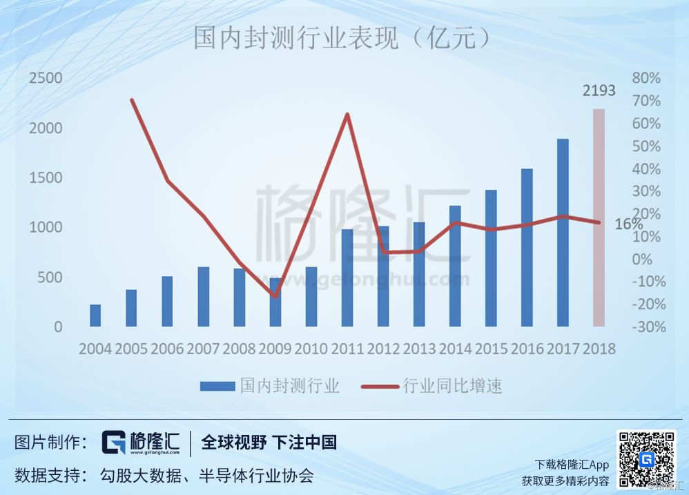
According to the statistics of China Semiconductor Industry Association, China's integrated circuit design industry, manufacturing industry and sealing and testing industry have achieved rapid growth in 2018. In 2018, the integrated circuit design industry achieved sales revenue of 251.93 billion yuan, an increase of 21.49 percent over the same period last year, the manufacturing industry achieved sales revenue of 181.82 billion yuan, an increase of 25.56 percent over the same period last year, and the sealing and testing industry achieved sales revenue of 219.39 billion yuan, an increase of 16.09 percent over the same period last year. The total sales revenue of the industry was 653.14 billion yuan, an increase of 20.69 percent over the same period last year.
The integrated circuit design industry accounts for 38% of the total output value of China's integrated circuit industry, manufacturing accounts for 27%, and closed testing accounts for 33%.
1.2 in the next 7 years, the growth rate of China's closed testing industry is about twice that of the world, reaching 12%.
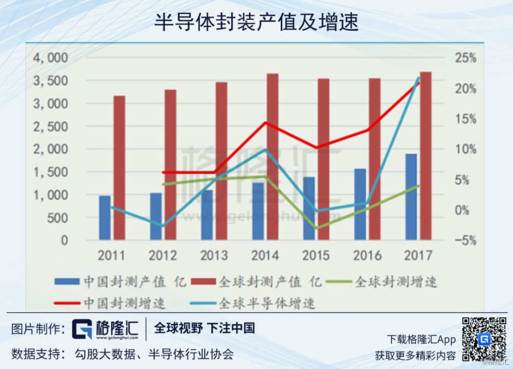
In 2018, the growth rate of China's closed testing industry reached 16%, and the packaging and testing industry accounted for 33% of the total sales revenue of China's integrated circuit industry. The global growth rate is only 4%. According to different chip types, chip closed testing can be divided into memory chip closed testing and logic chip closed testing. We expect the compound growth rate of the logic closed testing industry to reach 12% in the next 7 years, which is about twice that of the global logic closed testing industry.
The self-sufficiency rate of China's logic packaging and testing industry has increased from 42% in 2018 to about 52% in 2025, and its global market share will increase from 22% in 2018 to about 32% in 2025.
1.3 Global market competition pattern
In 2017, Sun and Moon acquired Silicon products, and the two companies together accounted for 30% of the global market share. China's Changdian Technology has also become the third largest closed testing company with a global market share of 13% through the acquisition of Xingke Jinpeng.

1.4 Evolution and trend of IC Packaging Technology
The evolution of integrated circuit packaging technology is mainly to meet the needs of terminal system products, in order to meet the development trend of multi-task and small volume of system products, the evolution direction of integrated circuit packaging technology is high density, high foot position, thinness and miniaturization. The development of IC packaging technology can be divided into four stages: the first stage: Jack original era; the second stage: surface mount era; the third stage: area array packaging era; the fourth stage: high-density system-level packaging era. At present, the mainstream of global semiconductor packaging is in the third stage of maturity, the main packaging technologies such as FC, QFN, BGA and WLCSP are produced on a large scale, and some products have begun to develop to the fourth stage.
With the acceleration of the Internet of things and the further development of a variety of smart wearable devices to miniaturization and multi-function, the chip size is becoming smaller and smaller, at the same time, there are more and more types of chips, and the number of input and output pins is also greatly increased. All kinds of advanced packaging technologies, such as 3D packaging, silicon perforation (TSV, Through Silicon Via), sector packaging (Fan-out wafer level packaging), wafer packaging fine pitch bonding (Wafer on wafer fine-pitch bonding), system packaging (Sip) and so on, have become the best choice to continue Moore's law.
The closed testing industry has evolved from the original cost-driven development to technology-driven development, and the advanced packaging field has become a strategic highland for the major closed test manufacturers to compete for layout. According to the data released by the international consulting firm Yole Development, the global advanced packaging market was close to US $25 billion in 2017, accounting for nearly 50% of the global closed test output value of 53 billion.
According to the share growth of different technology platforms, the chip flip FC (Flip Chip) closed test with the largest proportion has the highest output value, with a scale of about US $21 billion, and the future industry growth rate will be 7%. The growth rate of fan-in package (Fan-in) is similar to that of FC. The areas with faster growth in the future are mainly fan-out (Fan-out) and silicon through-hole (TSV) packaging technology. although the proportion is not high at present, the growth rate of the former is 15% in the next 6 years, while the growth rate of the latter is as high as 29%.
The manufacturers at the core of the advanced packaging market are mainly concentrated in Taiwan and the United States, with the closed test leader Sun-Moon / Silicon products accounting for 19.3%. Intel Corp Intel occupies the second place in the advanced packaging field, about 12.4%. The domestic closed test leader Changdian Technology leapt to the third place after the acquisition of Star Jinpeng, with a market share of 7.8%.

1.5. The driving force of the closed testing industry:SIP and fan-out
1) SIP: the driving force of the closed testing industry driven by the Internet of things and memory chips
The global semiconductor manufacturing process is approaching the physical limit of diodes, and the most advanced process is 7nm. Due to the huge investment, it becomes more and more expensive to further improve the performance of the chip from the manufacturing side. From the aspect of chip packaging, system-level packaging technology SIP can reduce chip size, improve chip performance and reduce power consumption by encapsulating chips with different functions, such as logic chip, memory memory, passive component IPD, RF RF and sensor, in one module.
Internet of things IOT (Internet of things) is an important application scenario to promote the development of SIP packaging technology. Wearable devices are the future application potential field of system-level packaging technology. Apple Watch fingerprint recognition sensor, 3D face recognition sensor, WiFi wireless network and other functional modules are packaged together, that is, the use of solar and moonlight system packaging (SiP) module technology Integrated circuits, discrete devices, optics, memory, multilayer ceramic capacitors and chip resistors are successfully integrated into thin and short substrates without interfering with each other. We believe that Apple Inc is at least one to two years ahead of competitors in the application of system packaging.
According to the complexity of different application requirements and products, system-level packaging SiP can be divided into 2D modules containing multiple active and passive components and more complex 3D modules, such as in-system packaging PiP (Package-in-Package), system-encapsulated PoP (Package-on-Package) and 2.5D/3D packaging technology. As the representative of 3D packaging technology, silicon through-hole technology TSV will be widely used in the field of 3D NANDFLASH flash memory packaging and DRAM memory packaging in the future.
Memory has become the most potential sub-section in the domestic semiconductor field. Two major memory projects, Changjiang Storage (NAND FLASH) and Hefei Changxin (DRAM), will be put into production in 2020, which will undoubtedly be a huge growth opportunity for domestic manufacturers with advanced packaging technology.
2) the closed test technology in the era of Fan-out:5G chip is very different.
Stepping into the 5G era, in order to obtain higher data transmission rate and bandwidth capacity, the electromagnetic wave with higher frequency must be used as the transmission medium, and the wavelength is shorter into the millimeter wave level. In the 5G era, the two mainstream frequencies, the Sub-6G Hz band and the 28GHz millimeter wave band, because the frequency increases, the wavelength decreases, the result is that the antenna is shorter, so the antenna is expected to be integrated into the chip to simplify the design and reduce the cost. There are two kinds of packaging technologies that may be used in the next generation of 5G chips: the on-chip antenna package AiP (Antenna in Package) with substrate and the fan-out package Fan-out without carrier board.
Because the second fan-out packaging scheme does not need a substrate, it can further reduce the cost and reduce the chip size on the basis of integrating multi-chips, so the fan-out packaging technology Fan-out is expected to become the mainstream technology of 5G chip packaging.
Among the manufacturers with fan-out packaging technology, the wafer foundry leader Taiwan Semiconductor Manufacturing Co Ltd TSMC has an obvious lead, and Taiwan's Sun and Moon and Licheng also have years of technology accumulation in the field of panel-level fan-out packaging. Among Chinese mainland closed test vendors, Changdian Technology has gained the lead in fan-out packaging technology after the acquisition of Jinke Xinpeng, and Huatian Technology has also been active in this field recently. On November 27, the silicon-based fan-out package of millimeter wave radar chip jointly developed by Kunshan Factory of Huatian Science and Technology Bulletin and Jiangsu Weiyuanxin Microsystem Technology Co., Ltd. has been successful, and the packaging rate of the product is more than 98%. At present, it has entered the stage of small batch production.

The packaging technology used in each electronic module in the automobile is different, in which the packaging of millimeter wave radar chips in automotive electronics will use a large number of Fan-out packaging technology. Domestic closed test factory director Dianke Jinpeng acquired eWLB packaging technology and became one of the earlier closed test manufacturers in the field of millimeter wave radar. Huatian Technology is expected to make a force in this field after making a technological breakthrough in the near future.
2
The situation of key listed companies
2.1 long-distance Technology (600584)
1) Company profile
The company's main business is the packaging and testing of integrated circuits and discrete devices, as well as chip design and manufacturing of discrete devices; to provide customers at home and abroad with a complete set of semiconductor packaging and testing solutions covering package design, solder bumps, needle testing, assembly, testing, distribution and so on. The company's main business model is to provide professional integrated circuit and discrete device packaging and testing services according to customer requirements and to process and sell discrete device packaging and testing products according to market demand.
Through the acquisition of Singapore Star Jinpeng in 2015, the company became the third in the global closed testing industry, and obtained a large number of overseas users of Starbucks Jinpeng, and expanded its business to the global market.
The contribution income of Xingke Jinpeng was 7.8 billion in 2016, accounting for 40.8% of the company's revenue in that year, and 7.8 billion yuan in 2017, accounting for 32.7% of the company's revenue.
At present, the company has production bases with clear division of labor, technical characteristics and competitive advantages in Singapore, South Korea, Jiangyin, Chuzhou and Suqian.
Company highlight 1:The national big fund is stationed.
On March 14, 2018, Changdian Technology plans to issue an additional 200 71.97 million shares and raise 4.05 billion matching funds. After the completion of the fixed increase, the Industrial Fund, Core Semiconductor and New Fashion Group became the top three shareholders of the company, with a shareholding ratio of 19%, 14.28%, 11.31% respectively.

Company highlight 2: the scale is the first in China, the third in the world


According to the IC Insights report, the sales revenue of Changdian Technology ranked third among the top 10 closed test plants of integrated circuits in the world in 2017. 80% of the world's top 20 semiconductor companies have become corporate customers.
Company highlight 3: master Fan-out eWLB and other advanced packaging technology
At present, the company's main products are QFN/DFN, BGA/LGA, FCBGA/LGA, FCOL, SiP, WLCSP, Bumping, MEMS, Fan-outeWLB, POP, PiP and traditional packaging SOP, SOT, DIP, TO and other series. The products are mainly used in computer, network communication, consumer electronics and intelligent mobile terminals, industrial automation control, power management, automotive electronics and other electronic and intelligent fields.

2) the financial situation of Changdian Science and Technology
In 2018, the company's revenue is expected to maintain 5% Mel 10% growth, profit according to the company's performance forecast loss of 950 million yuan, deducting non-loss of 1.3 billion yuan. The reason for the loss is the provision for impairment of receivables in a large scale.


2.2 Huatian Technology (002185)
1) Company profile
Huatian Technology is mainly engaged in semiconductor integrated circuits, MEMS sensors, semiconductor components packaging and testing business. At present, the company's integrated circuit packaging products are mainly DIP/SDIP, SOT, SOP, SSOP, TSSOP/ETSSOP, QFP/TQFP, QFN/DFN, BGA/LGA, FC, MCM (MCP), SIP, WLP, TSV, Bumping, MEMS and other series, the products are mainly used in computers, network communications, consumer electronics and intelligent mobile terminals, Internet of things, industrial automation control, automotive electronics and other electronic machines and intelligent fields.
At present, the company's main factories are located in Tianshui, Gansu, Xi'an, Shaanxi and Kunshan, Suzhou. In 2017, Tianshui Waterworks contributed 3.5 billion of revenue, accounting for about 50%, while Huatian Xi'an contributed more than 2.6 billion, accounting for about 37%. Suzhou Kunshan plant contributed 788 million revenue, accounting for about 11%.
From the perspective of revenue growth of various business lines, the fastest growth is Xi'an plant, which has grown by more than 30% in the past three years. Tianshui plant has a relatively stable growth because its business is mainly based on mature packaging technology. The growth rate of the Kunshan plant has declined significantly, falling from 24% in 2017 to 11% in the previous year and even a loss in mid-2018, mainly due to a 50% drop in the price of bumping products, low capacity utilization (60-70%) and high depreciation.

Xi'an plant: it is expected to replace Tianshui plant as a new revenue pillar in the future
Huatian Science and Technology Xi'an plant was officially put into operation in 2012, and began a period of rapid growth after it turned a profit the following year, with a compound revenue growth rate of 62% in 2011-2017, accounting for 37% of revenue in 2017. Over the past five years, the compound growth rate of net profit has been as high as 60%, and the profit share has increased from 17% in 2012 to 41% in 2017, making it an important core of the company's profit contribution.
At present, Xi'an factory packaging technology positioning is very clear, focusing on flip FC,BGA and LGA and other high-end packaging technology, the current core products include radio frequency power amplifier (PA), fingerprint chip, MCU, NOR FLASH flash memory chip (Zhaoyi, Wuhan Xinxin) and micro-electromechanical system (MEMS).
Kunshan factory
Huatian Technology Kunshan Factory, formerly known as Kunshan Xiti Microelectronics Co., Ltd., was established in June 2008. as the world's leading wafer-level packaging company, Huatian Technology Kunshan Factory has three supporting projects: wafer-level chip package TSV, wafer-level optical lens WLO and wafer-level camera module WLC.
At present, the company already holds a 93 per cent stake in the Kunshan plant, but the revenue growth of the Kunshan plant has been low in the past five years, with a compound revenue growth rate of only 4 per cent from 2012 to 2017, and net profit has been maintained at around 30 million.
Kunshan Factory is the main position of wafer-level packaging, focusing on advanced packaging technologies such as silicon through-hole TSV, bump packaging bumping and fan-out packaging fan-out. The main packaging products include security and automotive image sensor chips (CIS), mobile phone fingerprint chips and automotive millimeter wave radar chips. At present, Kunshan plant has a TSV production capacity of 23k pieces / month, bumping production capacity of 40k pieces / month, but bumping capacity utilization is low, fan-out is also in the capacity and yield climbing stage.
Nanjing factory
The Huatian Nanjing Plant under construction is expected to become the most important strategic layout of the company in the next 5-10 years.
In July 2018, the company announced an investment of 8 billion yuan in the new integrated circuit advanced closed testing industry base in Nanjing-Huatian Nanjing Plant, which has become another major layout of the company after Tianshui, Xi'an and Kunshan. The whole project is divided into three phases, all of which are scheduled to be completed and put into operation no later than December 31, 2028. At present, the first phase of the project is still in the plant design stage, and according to the general construction cycle of the integrated circuit project of about one and a half years, it is expected to start production and operation in mid-2020.
From the perspective of packaging products, the company announced that Nanjing Factory mainly carries out the packaging testing of integrated circuit products such as memory, MEMS, artificial intelligence and so on. The Yangtze River Delta region is the most mature region of the domestic integrated circuit industry. Not only does Ziguang Group layout the NAND FLASH flash memory project in Nanjing, but also the global wafer foundry leader Taiwan Semiconductor Manufacturing Co Ltd has also set up a factory in Nanjing. Nanjing is expected to become another important city of the global integrated circuit industry in the future.

2) the financial situation of Huatian Technology
In 2018, the company announced that in 2018, affected by the decline in the prosperity of the industry, the company achieved revenue of 7.1 billion, an increase of 1.45% over the same period last year, and net profit belonging to the shareholders of the parent company reached 387 million, down 22% from the same period last year.
In the first quarter of 2019, the company's performance forecast shows that net profit continues to decline, and Q1 net profit is expected to decline by 60% muri 90%, corresponding to a range of 8.13 million yuan to 32.52 million yuan.


3
Pay attention to the investment opportunities under the opportunity of the rise of semiconductors in China
At present, China is focusing on the manufacturing industry in the field of semiconductors. We account for only 11% of the world's wafer foundry, with annual imports of about US $200 billion. As a closed testing industry in the downstream field of semiconductors, well-known domestic and overseas companies have set up factories in China one after another, ushering in relatively certain opportunities for development.
Capacity construction of key wafer foundry in China:
